What is RAM?:
What is RAM? -Unlike ROM, we can read from or write into the RAM, so it is often called read/write memory. The numerical and character data that are to be processed by the computer change frequently. These data must be stored in type of memory from which they can be read by the microprocessor, modified through processing, and written back for storage. For this reason, they are stored in RAM instead of ROM. But it is a volatile memory, i.e. it cannot hold data when power is turned off.
There are two Types of RAM:
- Static RAM
- Dynamic RAM
Static RAM:
Most of the static RAM Architecture are built using MOS technology, but some are built using bipolar technology. In this section we will see both the types.
TTL RAM CELL:
Fig. 3.73 shows a simplified schematic of a bipolar memory cell. The memory cell is implemented using TTL (Transistor- Transistor-Logic) multiple emitter technology. It stores 1 bit of information. It is nothing but a flip-flop. It can store either 0 or 1 as long as power is applied, and it can set or reset to store either 1 or 0, respectively.
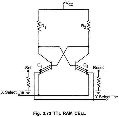
Operation:
The X select and Y select input lines select a cell from matrix. The Q1 and Q2 are cross coupled inverters, hence one is always OFF while the other is ON. A “1” is stored in the cell if Q1 is conducting and Q2 is OFF. A “0” is stored in the cell if Q2 is conducting and Q1 is OFF. The state of the cell is changed to a “0” by pulsing a HIGH on the Q1 (SET) emitter. This turns OFF Q1. When Q1 is turned OFF, Q2 is turned ON. As long as Q2 is ON, its collector is LOW and Q1 is held OFF.
A 1 can be rewritten by pulsing the Q2 (reset) emitter high. Large number of these memory cells are organized on a row and column basis to form a memory chip. Fig. 3.74 shows the row and column organization of a 8192 bit memory chip.
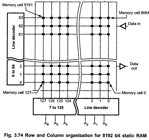
The chip has 13 address lines. The first seven address lines are connected to the column decoder to indicate one of the 128 columns. The remaining 6 address lines are connected to the row decoder to indicate one of 64 rows. Where the decoded row and column cross, they select the desired individual memory cell. Simple arithmetic shows that there are 64 x128=8192, crossings. Therefore, this memory has 8192 memory cells.
MOS Static RAM cell:
Fig. 3.75 shows a simplified schematic of MOS static RAM cell. Enhancement mode MOSFET transistors are used to make this RAM cell. It is very similar to TTL cell discussed earlier.
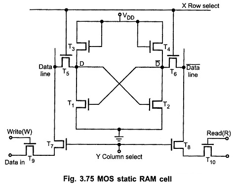
Here, T1 and T2 form the basic cross coupled inverters and T3 and T4 act as load resistors for T1 and T2. X and Y lines are used for addressing the cell. When X and Y both are high cell is selected. When X = 1, T5 and T6 get ON and the cell is connected to the data and data line. When Y = 1, T7 and T8 are made ON. Due to this, either read or write operation is possible.
Write Operation:
Write operation can be enabled by making W signal high. With write operation enabled, if data- in signal is logic 1, node D is also at logic 1. This turns ON T2 and T1 is cutoff. If new data on data-in pin is logic 0, T2 will be cutoff and T1 will be turned ON.
Read Operation:
Read operation can be enabled by making R signal high. With read operation enabled, T10 becomes ON. This connects the data output (Data) line to the data out and thus the complement of the bit stored in the cell is available at the output. Fig. 3.76 shows the organization MOS static RAM IC Intel 2167. It is 16 K x 1 RAM.
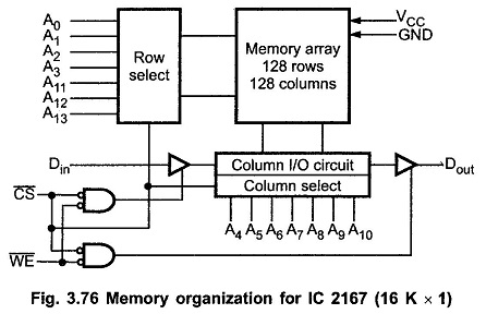
To enable Read and Write operation CS must be low. If CS and WE both are low, it is a write operation. In write operation, data on the Din input is written into the addressed cell while the output will remain in the high impedance state.
For Read operation CS signal must be low and WE signal must be high. In read operation, data from the addressed cell appears at the output while the input buffer is disabled.
When CS is high, both input and output buffers are disabled and the chip is effectively electrically disconnected. This makes the IC to operate in power down mode. In power down mode it takes only 40 mA current as compared to 125 mA in the active mode.
Dynamic RAM:
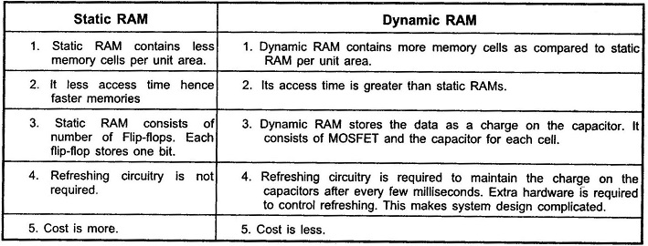
Dynamic RAM stores the data as a charge on the capacitor. Fig.3.77 shows the dynamic RAM cell. A dynamic RAM contains thousands of such memory cells. When COLUMN (Sence) and ROW (Control) lines go high, the MOSFET conducts and charges the capacitor. When the COLUMN and ROW lines go low, the MOSFET opens and the capacitor retains its charge. In this way, it stores 1 bit. Since only a single MOSFET and capacitor are needed, the dynamic RAM contains more memory cells as compared to static RAM per unit area.
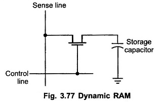
The disadvantage of dynamic RAM is that it needs refreshing of charge on the capacitor after every few milliseconds. This complicates the system design, since it requires the extra hardware to control refreshing of dynamic RAMs.
In this type of cell, the transistor acts as a switch. The basic simplified operation is illustrated in Fig. 3.78. As shown in the Fig. 3.78 circuit consists of three tri-state buffers : input buffer, output buffer and refresh buffer. Input and output buffers are enabled and disabled by controlling R/W line. When R/W line is LOW, input buffer is enabled and output buffer is disabled. When R/W line is HIGH, input buffer is disabled and output buffer is enabled. With this basic information let us see the read, write and refresh operations.
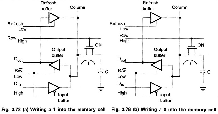
Write Operation:
To enable write operation R/W line is made LOW which enables input buffer and disables output buffers, as shown in the Fig. 3.78 (a). To write a 1 into the cell, the DIN line is HIGH, and the transistor is turned ON by a HIGH on the ROW line. This allows the capacitor to charge to a positive voltage. When 0 is to be stored, a LOW is applied to the DIN line. The capacitor remains uncharged, or if it is storing a 1, it discharges as indicated in Fig. 3.78 (b). When the ROW line is made LOW, the transistor turns off and disconnects the capacitor from the data line, thus storing the charge (either 1 or 0) on the capacitor.
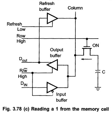
Read Operation:
To read data from the cell, the R/W line is made HIGH, which enables output buffer and disables input buffer. Then ROW line is made HIGH. It turns transistor ON and connects the capacitor to the DOUT line through output buffer. This is illustrated in Fig. 3.78 (c).
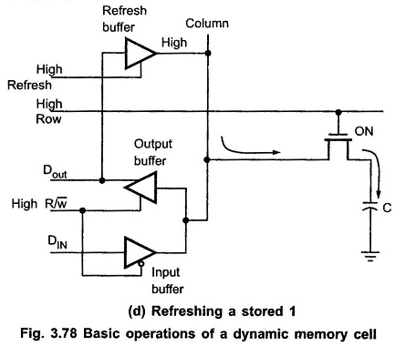
Refresh Operation:
To enable refresh operation R/W line, ROW line and REFRESH line are made HIGH. This turns ON transistor and connects capacitor to COLUMN line. As R/W is HIGH, output buffer is enabled and the stored data bit is applied to the input of refresh buffer. The enabled refresh buffer then produces a voltage on COLUMN line corresponding to the stored bit and thus replenishing the capacitor as shown in Fig. 3.78 (d).
Difference between Static RAM and Dynamic RAM:
In above discussion we have seen memory organization for ROM and Static RAM. In this organization, data is organized as a single bit data word. However, in most memory ICs the data is organized as eight bit data word. In these ICs eight memory cells are connected in parallel and enabled at a time to read or write eight bit data word. The eight memory cells connected in parallel forms a register and memory is nothing but an array of registers.
RAM Memory Structure and Its Requirements:
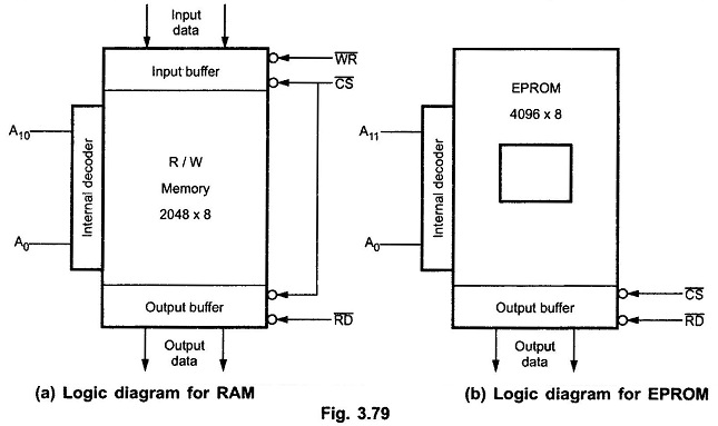
As mentioned earlier, read/write memories consist of an array of registers, in which each register has unique address. The size of the memory is N x M as shown in Fig. 3.79 (a) where N is the number of registers and M is the word length, in number of bits.