ADC0804 Family:
The ADC0804 Family are ADC0803, ADC0804 and ADC0805 are CMOS 8-bit successive-approximation analog to digital converters. These devices are design to operate from common microprocessor control buses, with tri-state output latches driving the data bus, and are identical except for accuracy.
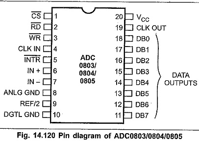
Pin Diagram of ADC0804 Family:
Fig. 14.120 shows the pin diagram of ADC0803, ADC0804 and ADC0805. IN+ and IN- inputs allow application of differential input voltage which has high common mode rejection and eliminates offset due to the zero input analog voltage value. The devices can operate with an external clock signal or, the on chip clock generator can be used independently by adding an external resistor and capacitor to set the time period.
Features of ADC0804 Family:
- 8-bit successive approximation ADC
- Conversion time 100 μs
- Access time 135 ns.
- It has an on-chip clock generator.
- It does not require any zero adjustment.
- It operate’s on single 5V power supply.
- Output meet TTL Output meet TTL voltage level specifications.
When the WR input goes low, the internal successive approximation register (SAR) is reset. As long as both CS and WR remain low, the analog to digital converter will remain in its reset state. One to eight clock periods after CS or WR makes a low-to-high transition, conversion starts. The INTR signal its held high during conversion process. After conversion, INTR goes low which is used as end of conversion signal. By making CS and RD signals low, an output can be read through DB0 to DB7 data signals.
Analog Inputs of ADC0804 Family:
As mentioned earlier, there are two analog inputs to ADC0803/0804/0805 : IN+ and IN-. These inputs are connected to an internal operational amplifier and are differential inputs. The differential input rejects the common mode noise and eliminates offset at zero analog input voltage.
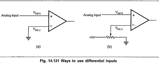
The Fig. 14.121 shows a few ways to use these differential inputs. The Fig 14.121 (a) shows the one way to use single input that can vary between 0V and +5V. Using another way variable voltage can be applied to the Vin, (—) pin so that the zero reference for Vin (+) can be adjusted, as shown in Fig. 14.121 (b).
Clock Signal:
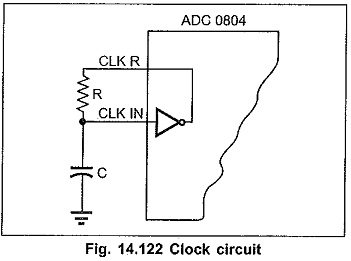
The ADC0803/0804/0805 requires a clock source ranging 100 kHz to 1460 kHz for operation. The clock signal can be applied external or it can be generated with an RC circuit, as shown in the Fig. 14.122. When the RC circuit, shown in Fig. 14.122 is used to generate the clock, the clock frequency is given as

Note : To have a minimum conversion time clock frequency should be kept nearer to 1460 kHz.
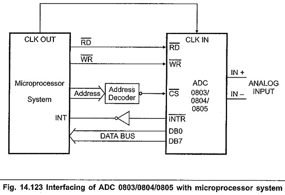
Typical Interface of ADC0804 Family:
Fig. 14.123 shows the interfacing of ADC 0803, ADC 0804 and ADC 0805 with microprocessor system.
Interfacing the ADC 0803/0804/0805 to 8086 Microprocessor:
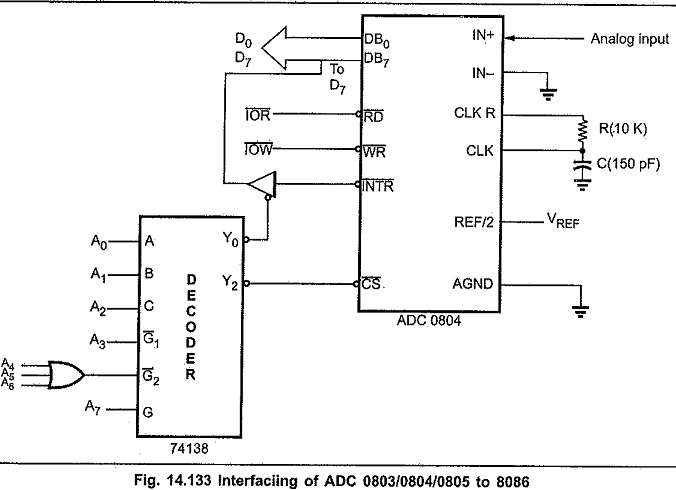
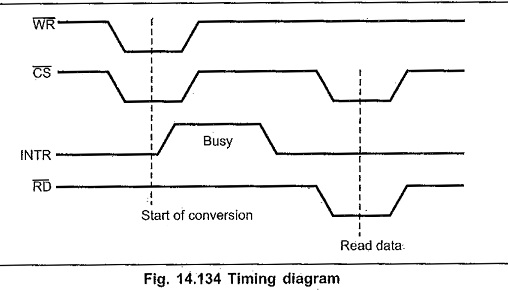
Fig. 14.133 shows the interfacing of ADC 0803/0804/0805 to the 8086 microprocessor. Here, converted digital data is read through data bus. The address is decoded using I/O mapped I/O technique. As shown in the Fig.14.133, address for ADC is 8011 The Fig. 14.134 shows the timing diagram of ADC operation. The conversion starts when CS and WR signals go low. The end of conversion is indicated by INTR output of the ADC. The INTR output goes low after conversion is over. Therefore, INTR signal is polled through data bus by enabling a buffer to detect the end of conversion. Once the conversion is over, the digital data is read by activating I/O read command. This is illustrated in the following procedure.
Interfacing ADC 0803/0804/0805 to 8086 using 8255:
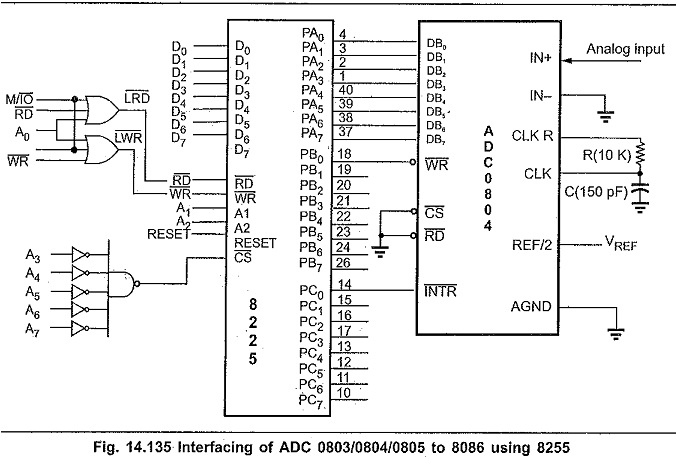
Fig. 14.135 shows the interfacing of ADC 0803/0804/0805 to 8086 using 8255. Here, port A of 8255 is used to read digital data from 8255. The start of conversion signal (WR and CS = low) generated using port B, PB0 pin. The end of conversion is detected by polling INTR pin through PC0.