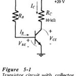
DC Load Line of BJT Biasing Circuit
DC Load Line of BJT Biasing Circuit: The DC Load Line of BJT Biasing Circuit is a straight line drawn on the transistor output characteristics. For a common-emitter (CE) circuit,…
Continue Reading
DC Load Line of BJT Biasing Circuit