Latching Circuit:
We know that AD0 to AD7 lines are multiplexed and the lower half of address (A0 – A7) is available only during T1 of the machine cycle. This lower half of address is also necessary during T2 and T3 of machine cycle to access specific location in memory or I/O port. This means that the lower half of an address bus must be latched in T1 of the machine cycle, so that it is available throughout the machine cycle. The Latching Circuit of lower half of an address is done by using external latch and ALE signal from 8085.
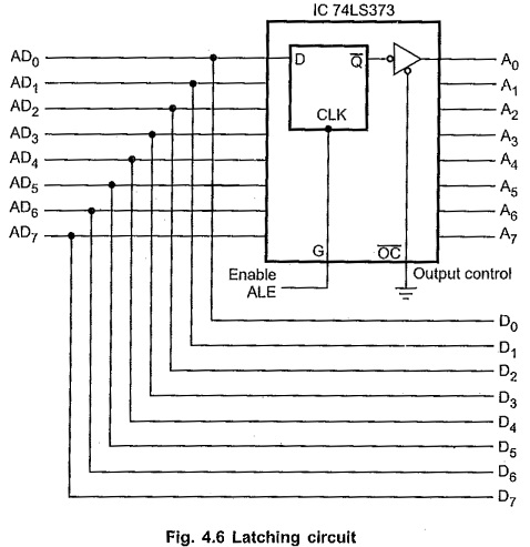
The Fig. 4.6 shows the hardware connection for Latching Circuit the lower half of an address. The IC 74LS373 is an 8-bit latch, having 8 D flip-flops. The input is transferred to the output only when clock is high. This clock signal is driven by ALE signal from 8085.
The ALE signal is activated only during T1, so input is transferred to the output only during T1 i.e. address (A0 – A7) on the AD0 to AD7 multiplexed bus. In the remaining part of the machine cycle, ALE signal is disabled so output of the latch (A0 – A7) remains unchanged.
To latch lower half of an address, in each machine cycle, the 8085 gives ALE signal high during T1 of every machine cycle.