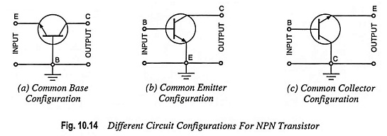
Transistor Circuit Configurations (CB, CE, CC)
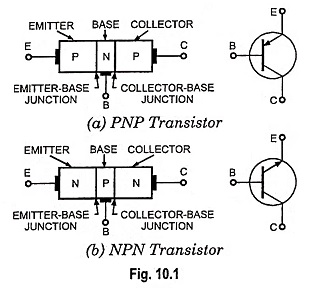
Transistor Circuit Configurations (CB, CE, CC): As already mentioned, a Transistor Circuit Configurations is a three-terminal device (having three terminals namely emitter, base and collector) but we require four terminals—two for the input and two…
Comments Off on Transistor Circuit Configurations (CB, CE, CC)
September 23, 2022