Transistor Operation:
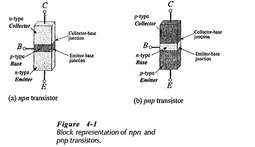
pnp and npn Transistor Operation – A junction transistor is simply a sandwich of one type of semiconductor material (p-type or n-type) between two layers of the opposite type. A block representation of a layer of p-type material between two layers of n-type is shown in Fig. 4-1(a). This is described as an npn transistor. Figure 4-1(b) shows a pnp transistor, consisting of a layer of n-type material between two layers of p-type. For reasons which will be understood later, the centre layer is called the base, one of the outer layers is termed the emitter, and the other outer layer is referred to as the collector. The emitter, base, and collector are provided with terminals which are appropriately labelled E, B, and C. Two pn-junctions exist within each transistor: the collector-base junction and the emitter-base junction.
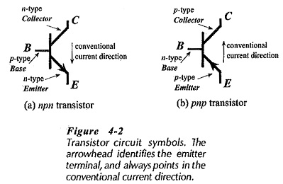
Circuit symbols for pnp and npn transistors are shown in Fig. 42. The arrowhead on each symbol identifies the transistor emitter terminal, and indicates the conventional direction of current flow. For an npn transistor, the arrowhead points from the p-type base to the n-type emitter. For a pnp device, the arrowhead points from the p-type emitter to the n-type base. Thus, the arrowhead always points from p to n.
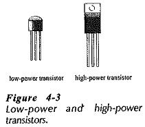
Two Transistor Operation packages are illustrated in Fig. 4-3; a low-power transistor, and a high power device. Low-power transistors typically pass currents of 1 mA to 20 mA. Current levels for high-power transistors range from 100 mA to several amps. The high-power Transistor Operation is designed for mechanical connection to a heat sink in order to prevent device overheating.
npn Transistor Operation:
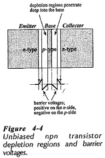
Figure 4-4 illustrates the depletion regions and barrier voltages at the junctions of an unbiased npn transistor. Although it is not shown in the illustration, the centre layer of the transistor is very much narrower than the two outer layers. Also, the outer layers are much more heavily doped than the centre layer, causing the depletion regions to penetrate deep into the base, as illustrated. Because of this penetration, the distance between the two depletion regions is very short (within the base). Note that the junction barrier voltages are positive on the emitter and collector, and negative on the base of the npn device.
Consider Fig. 4-5 which shows an npn Transistor Operation with external bias voltages. For normal operation, the base-emitter (BE) junction is forward biased and the collector-base (CB) junction is reverse biased. Note the external bias voltage polarities, The forward bias at the BE junction reduces the barrier voltage and causes electrons to flow from the n-type emitter to the p-type base. The electrons are emitted into the base region; hence the name emitter. Holes also flow from the p-type base to the n-type emitter, but because the base is much more lightly doped than the collector, almost all of the current flow across the BE junction consists of electrons entering the base from the emitter. Thus, electrons are the majority charge carriers in an npn device.
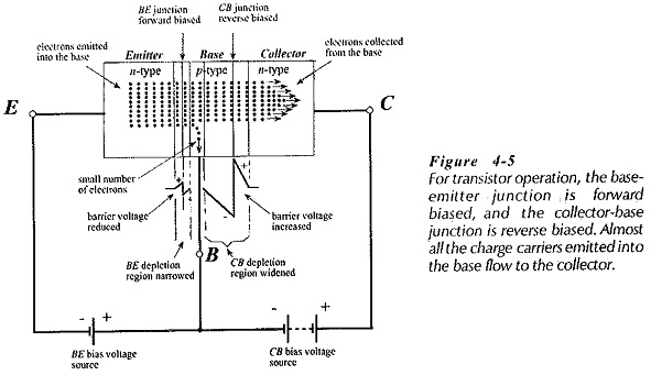
The reverse bias at the CB junction causes the CB depletion region to penetrate deeper into the base than when the junction is unbiased, (see Fig. 4 5). The electrons crossing from the emitter to the base arrive quite close to the large negative-positive electric field (or barrier voltage) at the CB depletion region. Because electrons have a negative charge, they are drawn across the CB junction by this bias voltage. They are said to be collected.
Some of the charge carriers entering the base from the emitter do not reach the collector, but flow out via the base connection, as illustrated in Fig. 4-5. However, the path from the BE junction to the CB depletion region is much shorter than that to the base terminal. So, only a very small percentage of the total charge carriers flow out of the base terminal. Also, because the base region is very lightly doped, there are few holes in the base to recombine with electrons from the emitter. The result is that about 98% of the charge carriers from the emitter are drawn across the CB junction to flow via the collector terminal and the voltage sources back to the emitter.
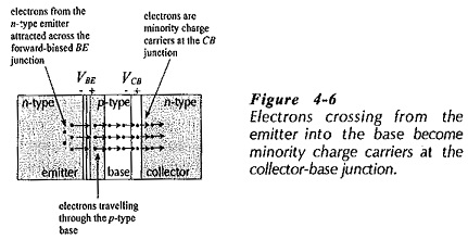
Another way of looking at the effect of the reverse-biased CB junction is from the point of view of minority and majority charge carriers. It has already been shown that a reverse-biased junction opposes the flow of majority charge earners and assists the flow of minority carriers. Majority carriers are, of course, holes from the p-side of a junction and electrons from the n-side. Minority carriers are holes from the n-side and electron from the Aside, (see Fig. 4-6). In the case of an npn transistor, the charge carriers arriving at the CB junction are electrons (from the emitter) travelling through the p-type base. Consequently, to the CB junction the appear a minority charge carriers, and the reverse bias assists them to cross the junction.
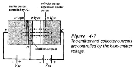
Because the BE junction is forward biased, it has the characteristics of a forward-biased diode. Substantial current will not flow until the forward bias is about 0.7 V for a silicon device, or about 0.3 V for germanium. Reducing the level of the BE bias voltage reduces the pn-junction forward bias, and thus reduces the current that flows from the emitter through the base to the collector. Increasing the BE bias voltage increases this current. Decreasing the BE bias voltage to zero, or reversing it, cuts the current off completely. Thus, variation of the small forward-bias voltage on the BE junction controls the emitter and collector currents, and the BE controlling voltage source has to supply only the small base current. This is illustrated in Fig. 4-7.
pnp Transistor Operation:
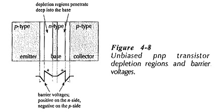
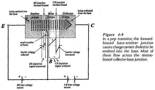
In an unbiased pnp transistor, the barrier voltages are positive on the base and negative on the emitter and collector, (see Fig. 4-8). As in the case of the npn device, the collector and emitter are heavily-doped, so that the BE and CB depletion regions penetrate deep into the lightly-doped base.
A pnp transistor behaves exactly the same as an npn device, with the exception that the majority charge carriers are holes. As illustrated in Fig. 4-9, the BE junction is forward biased by an external voltage source, and the CB junction is reverse biased. Holes are emitted from the p-type emitter across the forward-biased BE junction into the base. In the lightly doped n-type base, the holes find few electrons to absorb. Some of the holes flow out via the base terminal, but most are drawn across to the collector by the positive-negative electric field at the reverse-biased CB junction. Variation of the forward bias voltage at the BE junction controls the small base current and the much larger collector and emitter currents.
Bipolar Devices:
Although one type of charge carrier is in the majority in a pnp or npn transistor, two types of charge carrier (holes and electrons) are involved in the current flow. Consequently, these devices are termed bipolar junction transistors (BJT). This is to distinguish them from field-effect transistors (FET), which are termed unipolar devices, because they use only one type of charge carrier.
Summary:
A transistor is a sandwich of npn or pnp semiconductor materials. The outer layers are called the emitter and the collector, and the centre layer is termed the base. Two pn-junctions are formed, with depletion regions and barrier voltages at each junction. The barrier voltages are negative on the p-side and positive on the n-side.
The base-emitter junction is forward biased, so that charge carriers are emitted into the base. The collector-base junction is reverse biased, and its depletion region penetrates deep into the base. The base section is made as narrow as possible so that charge carriers can easily move across from emitter to collector. The base is also lightly doped, so that few charge carriers are available to recombine with the majority charge carriers from the emitter. Most charge carriers from the emitter flow to the collector; few flow out through the base terminal. Variation of the base-emitter junction bias voltage alters the base, emitter, and collector currents.