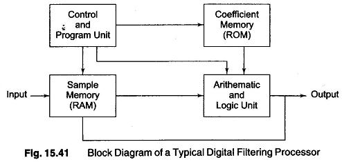
Block Diagram of a Digital Filtering Processor:
The implementation of any digital filtering consists of a series of multiplications of samples of the input and/or output signals by constants, and of the additions of these products. Thus the main building blocks which have to be present in digital filtering hardware are the following:
- Memory cells
- Adders
- Multipliers
- A programming unit which controls the sequence of operation
A general block diagram of a digital filtering processor is presented in Fig. 15.41. It is composed of the following.
- A memory for the input samples
- A memory for the output samples, if HR operations have to be performed
- A coefficient memory (ROM)
- ALU, which is capable of performing multiplications and additions
- Control unit for the control of the sequence of operation.
Several possibilities are now available for the implementation of the individual parts of this block diagram, which differ in speed of operation, level of integration, power consumption, etc. It is not possible to discuss all these possibilities, and all the structures which have been proposed for the implementation of digital filtering hardware.
The most general and powerful concept that needs to be considered is that of multiplexing. There are a lot of applications where it is necessary to process several low frequency signals in parallel, e.g. in the case of spectral analysis performed by means of a bank of filters on a low frequency signal. In this case, if a fast arithmetic unit is available, all the filtering operations can be performed with the same arithmetic unit, which is used sequentially to perform the operations required for these different filters.
Thus the processors for low frequency data can share the same arithmetic unit between all the necessary channels. In the opposite case, when the signal to be processed is a very high frequency one, the operations to be performed can be shared between different arithmetic units which work in parallel.
As far as the control part is concerned, two possibilities can be considered. The first is its implementation as a logical network which generates all the signals necessary to control the processor. The second is to use a microprogrammed structure, where the processing unit is constructed to accept a set of instructions, and sequences of such instructions are memorized on a suitable, generally high speed, memory and executed during processor operation. This method is much more flexible than the fixed network considered before, because here the basic structure can be reprogrammed if different operations have to be performed by the processor.