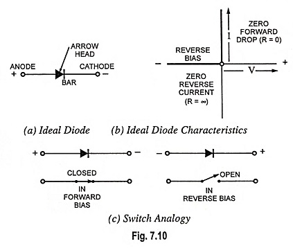
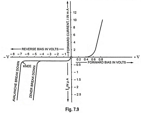
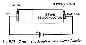
Determination of Diode Characteristics
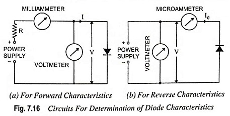
Determination of Diode Characteristics: Determination of Diode Characteristics - The forward characteristics of a diode can be obtained by use of the circuit depicted in Fig. 7.16 (a). The diode voltage is set at a…
Comments Off on Determination of Diode Characteristics
July 28, 2022