Tunnel Diode Operation and Characteristics:
Tunnel Diode Operation – A tunnel diode (sometimes called an Esaki diode after its inventor, Leo Esaki) is a two-terminal negative resistance device that can be employed as an amplifier, an oscillator, or a switch. Recall from earlier topics that the width of the depletion region at a pn-junction depends upon the doping density of the semi-conductor material.
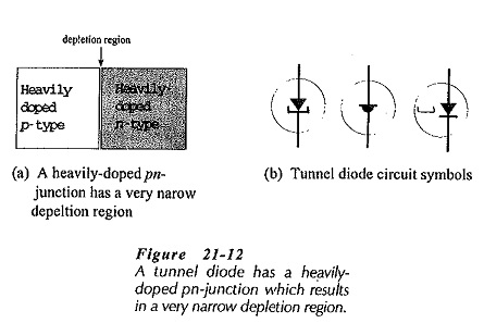
Lightly doped material has a wide depletion region, while heavily doped material has a narrow region. A Tunnel Diode Operation uses very heavily doped semiconductor material, so the depletion region is extremely narrow. This is illustrated in Fig. 21-12 along with three frequently-used tunnel diode circuit symbols.
The depletion region is an insulator because it lacks charge carriers, and usually charge carriers can cross it only when the external bias is large enough to overcome the barrier potential However, because the depletion region in a tunnel diode is so narrow, it does not constitute a large barrier to electron flow. Consequently, a small forward or reverse bias (not large enough to overcome the barrier potential) can give charge carriers sufficient energy to cross the depletion region. When this occurs, the charge carriers are said to be tunnelling through the barrier.
When a Tunnel Diode Operation junction is reverse biased, (negative on the p-side, positive on the n-side), substantial current flow occurs due to the tunnelling effect, (electrons moving from the p-side to the n-side). Increasing levels of reverse bias voltage produce more tunnelling and a greater reverse current. So, as shown in Fig. 21-13, the reverse characteristic of a tunnel diode is linear, just like that of a resistor.
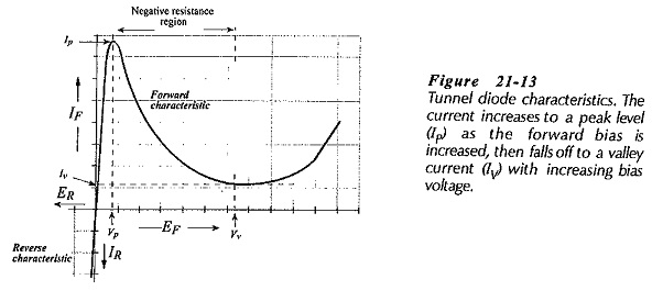
A forward biased Tunnel Diode Operation initially behaves like a reverse biased device. Electron tunnelling occurs from the n-side to the Aside, and the forward current (IF) continues to increase with increasing levels of forward voltage (EF). Eventually, a peak level of tunnelling is reached, and then further increase in EF, actually causes IF to decrease. (See the forward characteristic in Fig. 21-13.) The decrease in IF, with increasing EF, continues until the normal process of current flow across a forward biased junction begins to take over when the bias voltage becomes large enough to overcome the barrier potential. IF now commences to increase with increasing levels of EF, so that the final portion of the tunnel diode forward characteristics is similar to that for an ordinary prijunction. The shape of the tunnel diode characteristics can be explained in terms of energy band diagrams for the semiconductor material.
Characteristics and Parameters:
Consider the typical tunnel diode forward characteristics shown in Fig.21-14. The peak current (IP) and valley current (Iv) are easily identified on the forward characteristic as the maximum and minimum levels of IF prior to the junction being completely forward biased. The peak voltage (Vp) is the level of forward bias voltage (EF) corresponding to Ip, and the valley voltage (Vv) is the EF level at Iv. VF is the forward voltage drop when the device is completely forward biased. The dashed line at the bottom of the forward characteristic shows the characteristic for an ordinary forward biased diode. It is seen that this joins the Tunnel Diode Operation characteristic as VF is approached.
When a voltage is applied to a resistance, the current normally increases as the applied voltage is increased. Between IP and Iv on the tunnel diode characteristic, IF actually decreases as EF is increased. So, this region of the characteristic is named the negative resistance region, and the negative resistance (RD) of the tunnel diode is its most important property.
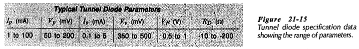
The negative resistance value can be determined as the reciprocal of the slope of the characteristic in the negative resistance region. From Fig. 21-14, the negative resistance is RD = Δ VF/Δ IF, and the negative conductance is GD = Δ IF/Δ VF. If RD is measured at different points on the negative resistance portion of the characteristic, slightly different values will be obtained at each point because the slope is not constant. Therefore, RD is usually specified at the center of the negative resistance region. Figure 21-15 lists typical tunnel diode parameters.
It is shown earlier that a straight-line approximation of diode characteristics can sometimes be conveniently employed. For a tunnel diode, the piecewise linear characteristics can usually be constructed from data provided by the device manufacturer.