Sample and Hold Circuit:
Four basic sample and hold circuit are shown in Fig. 14.141. In these circuits a JFET is used as switch. During the sampling time the JFET switch is turned on, and the holding capacitor charges up to the level of the analog input voltage. At the end of this short sampling period, the JFET switch is turned off. This isolates the holding capacitor. CH from the input signal. As a result, the voltage across capacitor CH and hence the output voltage will remain essentially constant at the value of the input voltage at the end of the sampling time. However, there will be a small drop-off or drop of the capacitor voltage during the hold period due to the various leakage currents. To avoid this, input and output buffers (voltage follower) circuits are used.
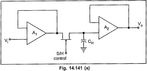
Fig. 14.141 (a) shows the open loop architecture of the sample and hold circuit. Remaining Figs show the closed loop architecture of the sample and hold circuit. Open loop type sample and hold circuits are faster than closed loop types which have delayed output fedback to the input buffer. However, closed loop architectures provide higher dc accuracy because of this feedback, cancelling the output amplifier offset errors.
The acquisition time of a S/H circuit is the time required for the holding capacitor CH to charge up to a level close to the input voltage during sampling. The acquisition time for S/H circuit should be as low as possible. In the circuit of Fig. 14.141 (a) there are three principle factors that will control the acquisition time.
These factors are :
- RC time constant where R is the rds (ON), i.e. on resistance of JFET and C is the holding capacitance CH.
- Maximum output current, which can be source or sunk by the operational amplifier.
- Slew rate of the op-amp.
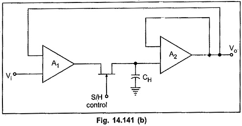
The circuit shown in Fig. 14.141 (b) offers some advantage over that of Fig. 14.141 (a) in terms of the acquisition time since the rds (ON) of the JFET switch is inside the feedback loop of A1 and A2. Therefore the acquisition time for this circuit is limited by maximum output current and slew rate of the op-amp, rather than the RC time constant.
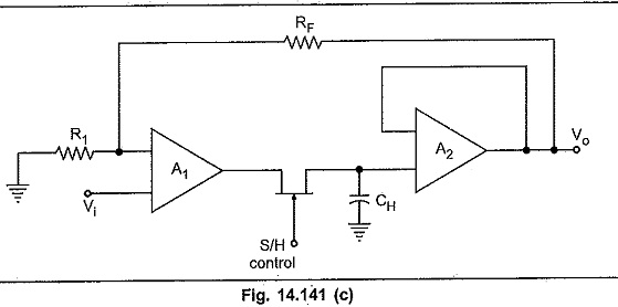
The S/H circuit of Fig. 14.141 (c) performs in a fashion similar to that of Fig. 14.141 (b) but it offers the additional feature of providing voltage gain. The voltage gain of this circuit can be given as A = 1 + (RF /R1). Therefore, the sampled output
advantage over that of Fig. 14.141 (a) in terms of the acquisition time since the rds (ON) of the JFET switch is inside the feedback loop of A1 and A2. Therefore the acquisition time for this circuit is limited by maximum output current and slew rate of the op-amp, rather than the RC time constant. voltage is equal to the sampled input voltage multiplied by the voltage gain factor of 1 + (RF /R1)
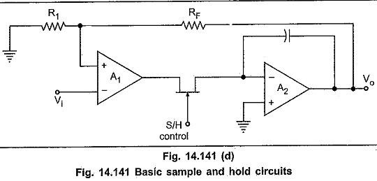
The S/H circuit of Fig. 14.141 (d) offers two advantages. The faster capacitor charging rate provides shorter acquisition time. This is because the voltage at the inverting input terminal of A2 is equal to the capacitor voltage divided by the open loop gain of A2. In this circuit, the summing input of A2 remains at virtual ground. Due to this, the charge removed from the summing junction via Cgd is constant regardless of the input and output signal levels. This removed charge appears as a constant offset at the output. However, as it is constant, it can be nulled by any standard offset trimming technique.
Performance Parameters of S/H Circuits:
The S/H circuit performance can be characterized by specifications of the ordinary amplifier such as input offset voltage, gain error, nonlinearity etc. However, during the transitions from one mode to other (sample to hold or hold to sample), as well as in hold mode, circuit performance is characterised by specifications peculiar to S/H circuits.
These specifications are explained below with the help of S/H circuit waveform, shown in Fig. 14.142.
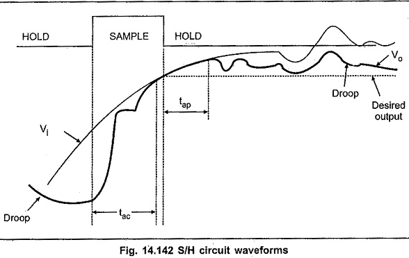
Acquisition time (tac):
It is the time required for the holding capacitor CH to charge up to a level close to the input voltage during sampling. It depends on three factors :
- RC time constant
- Maximum output current of op-amp
- Slew rate of op-amp
Aperture time (tap):
Because of propagation delays, through the driver and switch, Vo will keep tracking Vi some time after the inception of the hold command. This is the aperture time. To get the precise timing, it is necessary to advance hold command by this amount.
Aperture uncertainty (Δ tap):
It is the variation in aperture time from sample to sample. Due to aperture uncertainty it is difficult to compensate aperture time by advancing hold command.
Hold mode settling time (ts):
After the application of hold command, it takes a certain amount of time for Vo to settle within a specified error band, such as 1%, 0.1% or 0.01%. This is the hold mode settling time.
Hold step:
Because of the parasitic switch capacitances, at the time of switching between sample to hold mode, there is an unwanted transfer of charge between the switch driver and CH. This changes the capacitor voltage and hence the output voltage, as shown in the Fig. 14.142. This changes in output voltage are referred to as hold step, pedestal error and sample to hold offset. The change in the output voltage can be related as given below

Feedthrough:
In the hold mode, because of stray capacitance across the switch, there is a small amount of ac coupling between Vo and Vi. This ac coupling causes output voltage to vary with variation in the input voltage. This is referred to as feedthrough and it is given as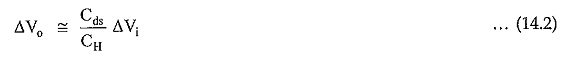
where Cds is the stray capacitance between drain and source of JFET.
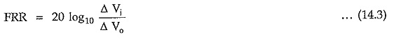
Feedthrough is usually expressed in terms of the feedthrough rejection ratio (FRR) and it is given as
Voltage drop:
The leakage current causes voltage of the capacitor to drop down. This is referred to as droop.
Advantages of Sample and Hold Circuit:
- The primary use of the sample and hold circuit to hold the sampled analog input voltage constant during conversion time of A/D converter.
- In case of multichannel ADCs, synchronization can be achieved by sampling signals from all channels at the same time.
- It also reduces the crosstalk in the multiplexer.
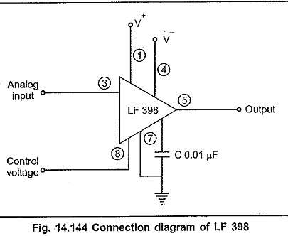
Sample and Hold Circuit using IC IF398:
For further improved performance, specially designed sample and hold circuit ic can be used: Such sample and hold ICs are HA 2420 by Harris Semiconductor, LF 198 and LF 398 by National Semiconductor. The very popularly Sample and Hold Circuit using IC IF398. The functional diagram of LF 398 is shown in the Fig. 14.143.
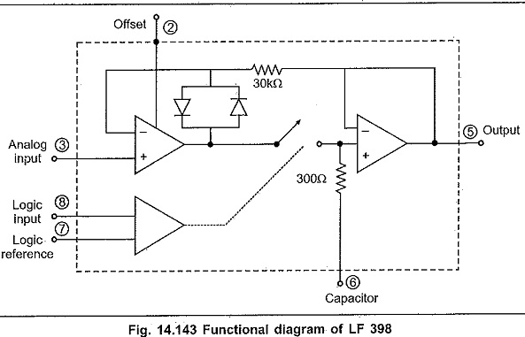
The hold or storage capacitor is required to be connected externally.
The connection diagram of LF 398 is shown in the Fig. 14.144.
Sample and Hold Circuit Applications:
The sample and hold circuit applications are :
- Digital interfacing.
- Analog to digital converter circuits.
- Pulse modulation systems.
- In storage of outputs of a multiplexer between updates in data distribution
- In reset-stabilised op-amps.
- In analog demultiplexers.