Quasi Complementary Output Stage:
The Quasi Complementary Output Stage was originally developed because complementary high-power transistors were not readily available. Despite the fact that such transistors are now available, the Quasi Complementary Output Stage circuit is still widely used.
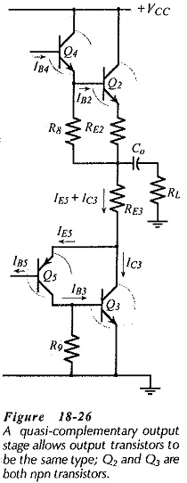
Consider the arrangement in Fig. 18-26. Q3 is a high-power npn transistor, and Q5 is a low-power pnp device. When Q5 base current (IB5) flows, the collector current of Q5 behaves (largely) as base current (IB3) for transistor Q3. This produces a Q3 collector current flow (IC3), which combines with IE5 to constitute a current flow in the load. Because IC3 ≫ IE5, the output current can be taken to be approximately IC3;
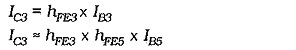
This is the same as the current gain with Darlington-connected transistors.
Now note that when a negative-going input voltage is applied to the base of Q5 a negative-going output occurs, because the emitter of Q5 (and the collector of Q3) follow the input voltage. Thus, the combination of transistors Q3 and Q5 in Fig. 18-26 behave as a high-power pnp emitter follower, just like Darlington-connected transistors Q3 and Q5.
Because transistors Q2 and Q3 in Fig. 18-26 are both npn devices, they can be the same type of transistor. This eliminates any problem with finding suitable complementary high-power transistors.
Resistor R9 In Fig. 18-26 ensures that Q3 is biased off when Q5 goes into cutoff.