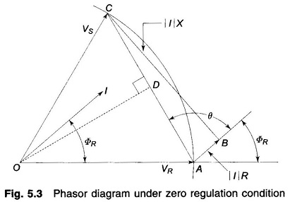
eeeguide

EEEGUIDE.COM - Online Electrical and Electronics Study

ROM Memory

ROM Memory

ROM Memory: It is a read only memory. We can’t write data in this ROM Memory. It is non-volatile memory i.e. it can hold data even if power is turned off. Generally, Read Only Memory is used to store the binary codes for the sequence of instructions you want the computer to carry out and

ROM Memory Read More »

What is Semiconductor Memory?

What is Semiconductor Memory

What is Semiconductor Memory?: What is Semiconductor Memory? – Memories are made up of registers. Each register in the memory is one storage location. Each location is identified by an address. The number of storage locations can vary from a few in some memories to hundreds of thousand in others. Each location can accommodate one

What is Semiconductor Memory? Read More »

Sequential Circuits

Block Diagram of Sequential Circuits

Sequential Circuits: There are many applications in which digital outputs are required to be generated in accordance with the sequence in which the input signals are received. This requirement cannot be satisfied using a combinational logic system. These applications require outputs to be generated that are not only dependent on the present input conditions but

Sequential Circuits Read More »

BCD Subtraction

BCD Subtraction: Addition of signed BCD numbers can be performed by using 9’s or 10’s complement methods. A negative BCD number can be expressed by taking the 9’s or 10’s complement. Let us see BCD Subtraction using 9’s Complement and BCD Subtraction using 10’s Complement numbers and BCD Subtraction process using it. 9s Complement: The

BCD Subtraction Read More »

BCD Adder Circuit

Decimal Adder BCD Adder

BCD Adder Circuit | BCD Adder Truth Table | BCD Adder Block Diagram: The digital systems handles the decimal number in the form of binary coded decimal numbers (BCD). A BCD Adder Circuit that adds two BCD digits and produces a sum digit also in BCD. BCD numbers use 10 digits, 0 to 9 which

BCD Adder Circuit Read More »

Combinational Circuit

Combinational Logic Circuit

Combinational Circuit | Block Diagram | Design Procedure: When logic gates are connected together to produce a specified output for certain specified combinations of input variables, with no storage involved, the resulting circuit is called Combinational Logic. In Combinational logic, the output variables are at all times dependent on the combination of input variables. A Combinational

Combinational Circuit Read More »

CMOS Inverter Working Principle

CMOS Inverter Circuit

CMOS Inverter Working Principle: CMOS Circuit contain both NMOS and PMOS devices to speed the switching of capacitive loads. It consumes low power and can be operated at high voltages, resulting in improved noise immunity. Fig. 3.1 shows the basic CMOS Inverter Working Principle. It consists of two MOSFETs in series in such a way that

CMOS Inverter Working Principle Read More »

Frequency Translator using PLL

Frequency Translator using PLL

Frequency Translator using PLL: The Frequency Translator means shifting the frequency of an oscillator by a small factor. Fig. 2.134 shows the block schematic for frequency translator using PLL. It consists of mixer, low pass filter and the PLL. The input frequency fs which has to be shifted is applied to the mixer. Another input

Frequency Translator using PLL Read More »

Scroll to Top