Op Amp Integrator Circuit:
In an Op Amp Integrator Circuit, the output voltage is the integration of the input voltage. The integrators circuit can be obtained without using active devices like op-amp, transistors etc. in such a case an integrator is called passive integrators. While an integrators using an active devices like op-amp is called active integrators. In this section, we will discuss the operation of active Op Amp Integrator Circuit.
Ideal Active Op-amp Integrator:
Consider the Op Amp Integrator Circuit as shown in the Fig. 2.35..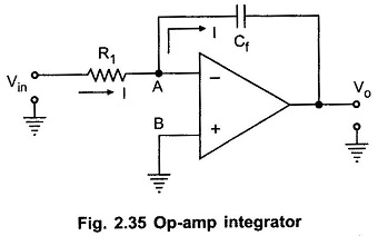
The node B is grounded. The node A is also at the ground potential from the concept of virtual ground
![]()
As input current of op-amp is zero, the entire current I flowing through R1, also flows through C f, as shown in the Fig. 2.35.
From input side we can write,
From output side we can write,
Equating the two equations (1) and (2)
Integrating both sides,
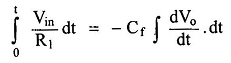
i.e.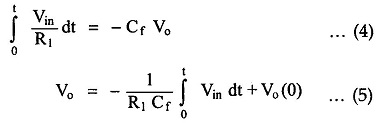
where Vo(0) is the constant of integration, indicating the initial output voltage.
The equation (5) shows that the output is -1/R1Cf times the integral of input and R1Cf is called time constant of the integrators.
The negative sign indicates that there is a phase shift of 180° between input and output. The main advantage of such an active integrators is the large time constant. By Miller’s theorem the effective capacitance between input terminal A and the ground becomes Cf (1-Av) where Av is the gain of the op-amp which is very large. Due to such large effective capacitance, time constant is very large and thus a perfect integration results due to such circuit.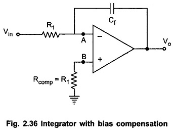
Sometimes a resistance Rcomp = R1 is connected to the noninverting terminal to provide the bias compensation. This is shown in the Fig. 2.36. As the input current of op-amp is zero, the node B is still can be treated at ground potential in this circuit. Hence the above analysis is equally applicable to the integrators circuit with bias compensation. And the output is the perfect integration of the input.
Input and Output Waveforms:
Let us see the output waveforms, for various input signals. For simplicity of understanding, assume that the time constant R1Cf = 1 and the initial voltage Vo(0) = 0V.
i) Step input signal:
Let the input waveform is of step type, with a magnitude of A units as shown in the Fig. 2.37.
Mathematically the step input can be expressed as,
From equation (5), with R1Cf = 1 and Vo(0) = 0,
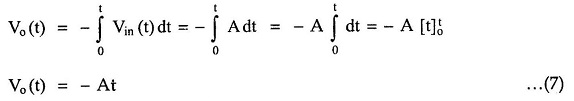
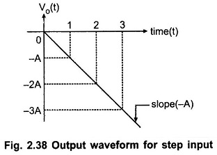
Thus output waveform is a straight line with a slope of -A where A is magnitude of the step input. The output waveform is shown in the Fig. 2.38.
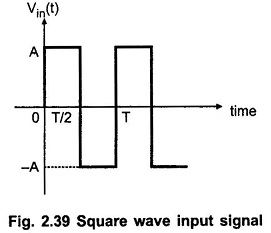
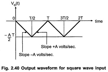
ii) Square wave input signal:
Let the input waveform is a square wave as shown in the Fig. 2.39. It can be observed that the square wave is made up of steps i.e. a step of A between time period of 0 to T/2 while a step of – A units between a time period of T/2 to T and so on.
Mathematically it can be expressed as,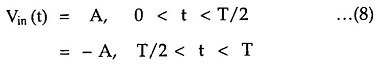
This is the expression for the input signal for one period.
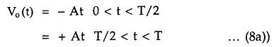
As discussed earlier, the output for step input is a straight line with a slope of – A. So for the period 0 to T/2 output will be straight line with slope – A. From t = T/2 till t = T, the slope of the straight line will become – (- A) i.e. + A. So the output can be expressed mathematically for one period as,
The output waveform is shown in the Fig. 2.40.
iii) Sine wave input signal:
Let the input waveform is purely sinusoidal with a frequency of ω rad/sec. Mathematically it can be expressed as,
![]()
where Vm is the amplitude of the sine wave and T be the period of the waveform.
To find the output waveform, use the equation (5) with R1Cf = 1 and Vo(0) = 0V.
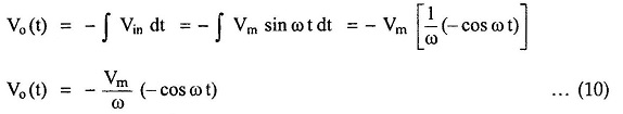
Thus it can be seen that the output of an integrators is a cosine waveform for a input. Due to inverting integrators, the output waveform is as shown in the Fig. 2.41.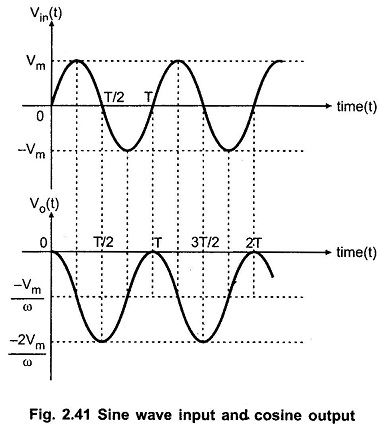
Errors in an Ideal Integrator:
The operation amplifier has input offset voltage (Vios) and the input bias current (Ib). In the absence of input voltage or at zero frequency (d.c.), op-amp gain is very high. The input offset voltage gets amplified and appears at the output as an error voltage. The bias current also results in a capacitor charging current and adds its effect in an output error voltage. The two components, due to high d.c. gain of op-amp cause output to ramp up or down, depending upon the polarities of offset voltage and/or bias current. After some time, output of op-amp may achieve its saturation level. Hence there is a possibility of op-amp saturation due to such an error voltage and it is very difficult to pull op-amp out of saturation. Thus the output of an ideal integrators in the absence of input signal is likely to be offset towards the positive or negative saturation levels.
In the presence of the input signal also, the two components namely offset voltage and bias current, contribute an error voltage at the output. Thus it is not possible to get a true integration of the input signal at the output. Output waveform may be distorted due to such an error voltage.
Another limitation of an ideal integrators is its bandwidth, which is very small. Hence an ideal integrator can be used for a very small frequency range of the input only.
Due to all these limitations, an ideal integrators is not used in practice. Some additional components are used along with the basic integrator circuit to reduce the effect of an error voltage, in practice. Such an integrator is called Practical Integrators Circuit.
Practical Integrator:
The limitations of an ideal integrators can be minimized in the practical integrators circuit, which uses a resistance Rf in parallel with the capacitor Cf.
The practical integrators circuit is shown in the Fig. 2.42.
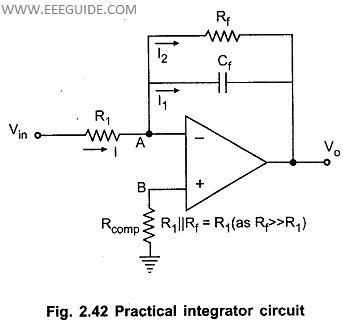
The resistance Rcomp is also used to overcome the errors due to the bias current. The resistance Rf reduces the low frequency gain of the op-amp
The Analysis of Practical Integrators:
As the input current of op-amp is zero, the node B is still at ground potential. Hence the node A is also at the ground potential from the concept of virtual ground. So VA =0.
Referring to Fig. 2.42,
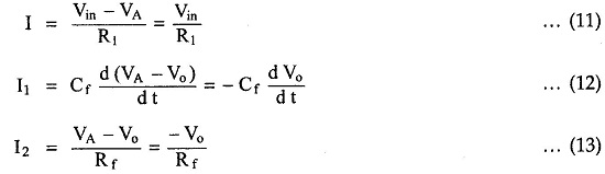
At node A, applying KCL
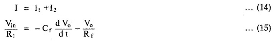
Taking Laplace of this equation,
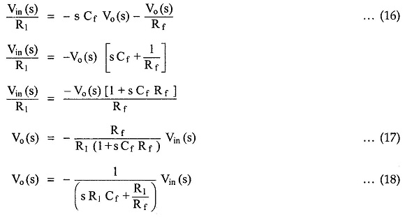
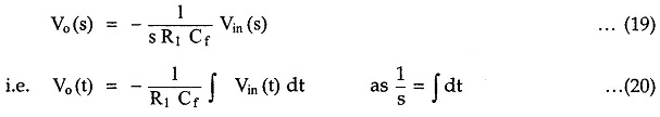
When Rf is very large then R1/Rf can be neglected and hence circuit behaves like an ideal integrator as
Application of Practical Integrator:
The Practical Integrator circuits are most commonly used in the following applications :
- In the analog computers.
- In solving the differential equations.
- In analog to digital converters.
- Various signal wave shaping circuits.
- In ramp generators.