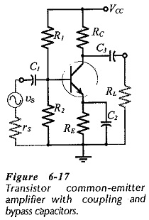
Common Emitter Amplifier Circuit:
Consider the Common Emitter Amplifier Circuit circuit shown in Fig. 6-17. When the capacitors are regarded as ac short-circuits, it is seen that the circuit input terminals are the transistor base and emitter, and the output terminals are the collector and the emitter. So, the emitter terminal is common to both input and output, and the circuit configuration is termed common-emitter (CE).
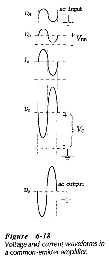
The current and voltage waveforms for the CE circuit in Fig. 6-17 are illustrated in Fig. 6-18. It is seen that there is a 180° phase shift between the input and output waveforms. This can be understood by considering the effect of a positive-going input signal. When υs increases in a positive direction, it increases the transistor base-emitter voltage (VBE). The increase in VBE raises the level of IC, thereby increasing the voltage drop across RC, and thus reducing the level of the collector voltage (VC). The changing level of VC is capacitor-coupled to the circuit output to produce the ac output voltage (υo). As υs increases in a positive direction, υo goes in a negative direction, as illustrated. Similarly, when υs changes in a negative direction, the resultant decrease in VBE reduces the IC level, thereby reducing VRC, and producing a positive-going output.
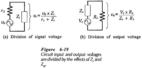
The circuit in Fig. 6-17 has an input impedance (Zi), and an output impedance (Zo). These can cause voltage division of the circuit input and output voltages, as illustrated in Fig. 6-19. So, for most transistor circuits, Zi and Zo are important parameters. The circuit voltage amplification (Aυ), or voltage gain, depends on the transistor parameters and on resistors RC and RL.
h-Parameter Equivalent Circuit:
The first step in ac analysis of a transistor circuit is to draw the ac equivalent circuit, by substituting short-circuits in place of the power supply and capacitors. When this is done for the circuit in Fig. 6-17, it gives the ac equivalent circuit shown in Fig. 6-20(a). The h-parameter circuit is now drawn simply by replacing the transistor in the ac equivalent circuit with its h-parameter model. This gives the CE h-parameter equivalent circuit in Fig. 6-20(b). Note that the feedback voltage generator (hreυc) is omitted in Fig. 6-20(b). As discussed, the effect of hreυc in a CE circuit is unimportant for most practical purposes.
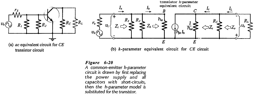
The current directions and voltage polarities in Fig. 6-20(b) are those that occur when the instantaneous level of the input voltage is moving in a positive direction.
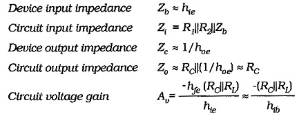
Input Impedance:
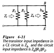
The input section of the h-parameter circuit in Fig. 6-20(b) reproduced in Fig. 6-21 shows that the input impedance at the transistor terminals is,
![]()
A typical value of hie for a low-current transistor is 1.5 kΩ. If hie is not known, it can be estimated by first calculating r′e from Eq. 6-2 or Eq. 6-3, as appropriate. Then r′e = hib, and hie = (1 + hfe)hib.
Zb is the input impedance at the device base terminal. At the circuit input terminals, resistors R1 and R2 are seen to be in parallel with Zb. So, the circuit input impedance is,
![]()
Output Impedance:
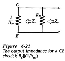
Looking into the output of the CE h-parameter circuit reproduced in Fig. 6-22, the output impedance at the transistor collector is,
![]()
At the circuit output terminals, resistor RC is in parallel with Zc. So, the circuit output impedance is,
![]()
Because 1/hoe is typically 50 kΩ and RC is usually much less than 50 kΩ, the circuit output impedance is approximately equal to RC. Using this information, it is possible to tell the output impedance of a CE circuit simply by reading the resistance of RC.
Voltage Gain:
The circuit voltage gain is given by the equation,
![]()
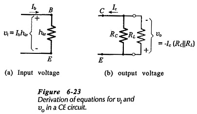
Figure 6-23(a) and (b) reproduced from Fig. 6-20 shows that,
IC/lb can be replaced with hfe. Also, because 1/ hoe can be omitted from the equation because it is usually much larger than RC||RL.
The normally used voltage gain equation now becomes,
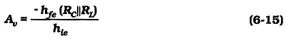
The minus sign in Eq. 6-15 indicates that υo is 180° out of phase with υi. (When υi increases, υo decreases, and vice versa.) Knowing the appropriate h-parameters as well as RC and RL the voltage gain of a CE circuit can be quickly estimated. Using values of RC = 4.7 kΩ. hfe = 70, hie = 1.5 kΩ, and assuming that RL≫RC, a typical CE voltage gain is -220.
Substituting from Table 6-1, the CE voltage gain equation can be rewritten as,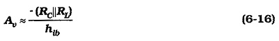
hib can be determined approximately as r’e from the emitter current level. So, Eq. 6-16 can be useful in cases where the device parameters are not known.
Current Gain:
The transistor current gain is,
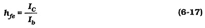
This is the device current gain, not the circuit current gain. Examination of the circuit in Fig. 6-20 shows that the signal current (Is) is divided between hie and the bias resistors [RB = (RC||RL)]. Also, that the output current from the transistor collector (Ic) is divided between RC and RL. The overall circuit current gain can be shown to be,
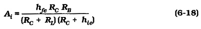
In virtually all practical applications, the current gain of a Common Emitter Amplifier Circuit is normally not an important quantity.
Power Gain:
The power gain of an amplifier can be shown to be,
![]()
Like current gain, the power gain of a Common Emitter Amplifier Circuit is largely unimportant for practical applications.
Summary of Typical CE Circuit Performance:
The Common Emitter Amplifier Circuit has good voltage gain, with 180° phase shift, medium input impedance, and relatively high output impedance. As a voltage amplifier, the CE circuit is by far the most often used of the three basic circuit configurations.