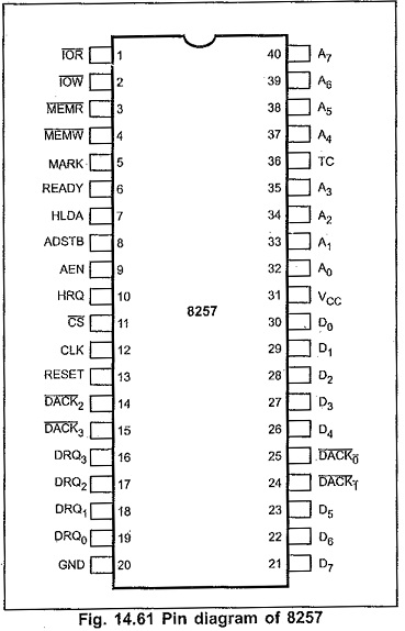
8257 Pin Diagram:
Fig. 14.61 shows 8257 Pin Diagram.
Data Bus (D0-D7) : These are bi-directional tri-state signals connected to the system data bus. When CPU is having control of system bus it can access contents of address register, status register, mode set register, and a terminal count register and it can also program, control registers of DMA controller, through the data bus.
During DMA cycles these lines are used to send the most significant bytes of the memory address from one of the
8257 Pin Description:
Address Bus (A0-A3 and A4-A7) : The four least significant lines A0-A3 are bi – directional tri – state signals. In the idle cycle they are inputs and used by the CPU to address the register to be loaded or read. In the Active cycle they output the lower 4 bits of the address for DMA operation. A4-A7 are unidirectional lines, provide 4-bits of address during DMA service.
Address Strobe (ADSTB) : This signal is used to demultiplex higher byte address and data using external latch.
Address Enable (AEN) : This active high signal enables the 8-bit latch containing the upper 8-address bits onto the system address bus. AEN can also be used to disable other system bus drivers during DMA transfers.
Memory Read and Memory Write ( MEMR, MEMW) : These are active low tri-state signals. The MEMR signal used to access data from the addressed memory location during a DMA read or memory-to-memory transfer and MEMW signal is used to write data to the addressed memory location during DMA write or memory to memory transfer.
I/O Read and I/O Write ( IOR and IOW ) : These are active low bi-directional signals. In idle cycle, these are an input control signals used by CPU to read/write the control registers. In the active cycle IOR signal is used to access data from a peripheral and IOW signal is used to send data to the peripheral.
Chip Select (CS) : This is an active low input, used to select the 8257 as an I/O device during the idle cycle. This allows CPU to communicate with 8257 Pin Diagram.
Reset : This active high signal clears, the command, status, request and temporary registers. It also clears the first/last flip-flop and sets the Master Register. After reset the device is in the idle cycle.
Ready : This input is used to extend the memory read and write signals from the 8257 to interface slow memories or I/O devices.
Hold request (HRQ) : Any valid DREQ causes 8257 to issue the HRQ. It is used for requesting CPU to get the control of system bus.
Hold Ackmiwledge (HLDA) : The active high Hold Acknowledge from the CPU indicates that it has relinquished control of the system bus.
DREQ0-DREQ3 : These are DMA request lines, which are activated to obtain DMA service, until the corresponding DACK signal goes active.
DACK0-DACK3 : These are used to indicate peripheral devices that the DMA request is granted.
Terminal Count (TC) : This is active high signal concern with the completion of DMA service. The TC output signal is activated at the end of DMA service, i.e. when present cycle is a last cycle for the current data block.
MARK : This output notifies the selected peripheral that the current DMA cycle is the 128th cycle since the previous MARK output. MARK always occurs at 128 (all multiplies of 128) cycles from the end of the data block.
8257 Block Diagram:
Fig. 14.62 shows the functional 8257 Block Diagram.
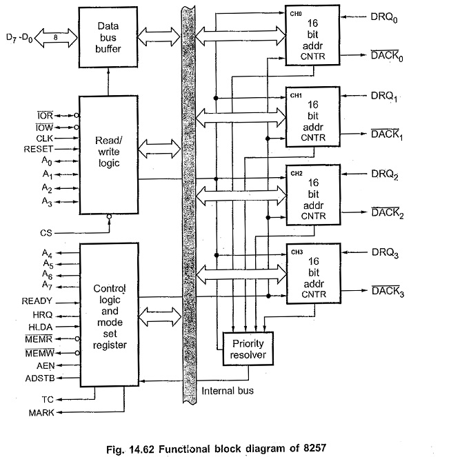
Data Bus Buffer:
It is a tri-state, bi-directional, eight bit buffer which interfaces the 8257 to the system data bus. In the slave mode, it is used to transfer data between microprocessor and internal registers of 8257. In master mode, it is used to send higher byte address (A8-A15) on the data bus.
Read/Write logic:
When the CPU is programming or reading one of the internal registers of 8257 Pin Diagram (i.e, when the 8257 is in the slave mode), the Read/Write logic accepts the I/O Read (IOR) or I/O Write (IOW) signal, decodes the the least significant four addiess bits (A0 – A3) and either writes the contents of the data bus into the addressed register (if IOW is low) or places the contents of the addressed register onto the data bus (if IOR is low).
During DMA cycles (i.e. when the 8257 is in the master mode) the Read/Write logic generates the I/O read and memory write (DMA write cycle ) or I/O write and memory read (DMA read cycle) signals which control the data transfer between peripheral and memory device.
8257 DMA Controller Operating Modes:
The 8257 Pin Diagram provides four identical channels, labeled CH0 to CH3. Each channel has two sixteen bit registers:
- A DMA address register, and
- A terminal count register.
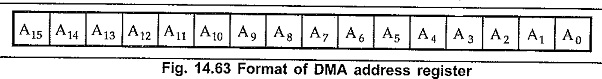
DMA address register : Fig. 14.63 shows the format of DMA address register. It specifies the address of the first memory location to be accessed. It is necessary to load valid memory address in the DMA address register before channel is enabled.
Terminal Count Register : Fig. 14.64 shows the format of Terminal Count register.
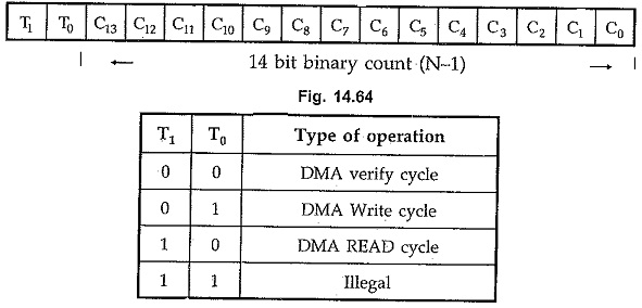
Note : N is number of bytes to be transferred.
The value loaded into the low order 14 bits (C13 — C0) of the terminal count register specifies the number of DMA cycles minus one before the terminal count (TC) output is activated. Therefore, for N number of desired DMA cycles it is necessary to load the value N-1 into the low order 14-bits of the terminal count register. The most significant 2 bits of the terminal count register specifies the type of DMA operation to be performed. It is necessary to load count for DMA cycles and operational code for valid DMA cycle in the terminal count register before channel is enabled.
Control logic:
It controls the sequence of operations during all DMA cycles (DMA read, DMA write, DMA verify) by generating the appiopriate control signals and the 16-bit address that specifies the memory location to be accessed. It consists of mode set register and status register. Mode set register is programmed by the CPU to configure 8257 whereas the status register is read by CPU to check which channels have reached a terminal count condition and status of update flag.
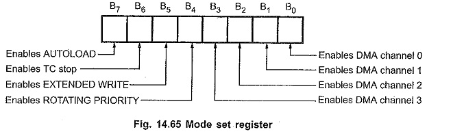
Mode Set Register:
Fig. 14.65 gives the format of mode set register. Least significant four bits of mode set register, when set, enable each of the four DMA channels. Most significant four bits allow four different options for the 8257 Pin Diagram.
It is normally programmed by the CPU after initializing the DMA address registers and terminal count registers. It is cleared by the RESET input, thus disabling all options, inhibiting all channels, and preventing bus conflicts on power-up.
Status Register:
Fig. 14.66 shows the status register format. As said earlier, it indicates which channels have reached a terminal count condition and includes the update flag described previously.
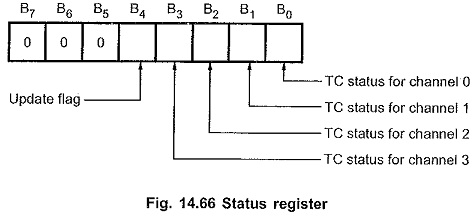
The TC status bit, if one, indicates terminal count has been reached for that channel. TC bit remains set until the status register is read or the 8257 is reset. The update flag, however, is not affected by a status read operation.
The update flag bit, if one, indicates CPU that 8257 is executing update cycle. In update cycle 8257 loads parameters in channel 3 to channel 2.
Priority Resolver:
It resolves the peripherals requests. It can be programmed to work in two modes, either in fixed mode or rotating priority mode.