Gate Turn Off Thyristor (GTO) – Symbol, Operations and Applications:
Conventional thyristors are used as ideal switches in power electronic applications. They have the capability of blocking several thousand volts in the off-state and conducting several thousand amperes in the on-state with only small on-state voltage drop. The only drawback of conventional thyristor is that when the gate turns into on-state, the gate loses the control over the device and, therefore, it cannot be turned off without the technique called commutation. The circuitry required for commutation makes the device costlier and bulky. This can be avoided by using a device of thyristor family, known as the gate turn-off thyristor (GTO).
A Gate Turn Off Thyristor like an SCR can be turned on by applying a positive gate signal. However, a GTO can be turned off by a negative gate signal. A GTO is a non-latching device and can be built with current and voltage ratings similar to those of an SCR. The device incorporates the character of both of a thyristor and a transistor.
The GTOs have the advantages over SCRs : (i) elimination of commutating components in forced commutation, resulting in reduction in cost, weight and volume (ii) faster turn-off permitting high switching frequencies (iii) improved efficiency of converters (iv) reduction in accoustic and electromagnetic noise due to elimination of commutation chokes (v) high blocking voltage and large current capability.
In low-power applications, GTOs have the following advantages over BJTs :
- Higher blocking voltage capability.
- High ratio of peak controllable current to average current.
- High ratio of peak surge current to average current, typically 10 : 1.
- High on-state gain (anode current and gate current) typically 600.
- Pulsed gate signal of short duration.
Under surge conditions, a GTO goes into deeper saturation due to regenerative action. On the other hand, a BJT tends to come out of saturation.
However, the GTO has the following disadvantages :
- High latching and holding currents.
- More on-state voltage drop and associated loss.
- Higher triggering gate current due to multi-cathode structure as compared to conventional thyristor.
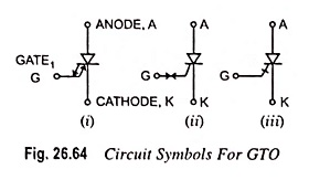
The symbols of Gate Turn Off Thyristor (GTO) are shown in Fig. 26.64.
The internal cross section of a Gate Turn Off Thyristor is shown in Fig. 26.65 (a). Compared to a conventional thyristor, it has an additional N+ -layer near the anode that forms a turn-off circuit between the gate and the cathode in parallel with the turn-on gate. The equivalent circuit is depicted in Fig. 26.65 (b) which is similar to that of a thyristor, except for its internal turn-off mechanism. If a large pulse current is passed from the cathode to the gate to take away sufficient charge carriers from the cathode i.e., from the emitter of the NPN transistor, the PNP transistor can be driven out of the regenerative action. As transistor NPN turns off, transistor PNP is left with open base, and the GTO returns to the nonconducting state.
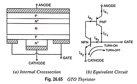
The two transistor analogy of a GTO shown in Fig. 26.65 (b) is the same as that of a conventional thyristor with the only difference that the gain of PNP transistor is reduced to a low value in this device. When a thyristor is turned on by using a positive gate pulse the collector currents of PNP as well as NPN transistors are high. Under such condition, the application of negative pulse to the gate terminal cannot reduce the collector current to such a value that NPN transistor may be pulled into cut off. The result is that the device does not turn off. However, in a GTO the collector current of PNP transistor is low. When a negative pulse is applied to its gate terminal, the collector current IC1 is diverted away from the base of NPN transistor. When current IB2 is reduced below threshold value the NPN transistor and therefore PNP transistor as well are turned off. Thus the device turns to off state. The current required to turn off the device is higher in case of GTO—the gate triggering current may be of the order of 20 mA and 30 μA respectively in case of GTO and a conventional thyristor.
The reduction in gain of the PNP transistor can be achieved by either of the two following techniques or by combination of both : One technique involves the diffusion of gold or other heavy metal to reduce the carrier lifetime. The other technique is introduction of anode to N-base short-circuiting spots. Device characteristics depend on the technique used. The gold-doped GTO retains its reverse blocking capacity and has a high on-state voltage drop. On the other hand, the shorted anode emitter construction has a lower on-state voltage, but it loses the ability to block reverse voltage.
Applications of Gate Turn Off Thyristor (GTO):
GTOs are mostly used in voltage-source converters in which a fast recovery antiparallel diode is required across each GTO. Thus, GTOs normally do not require reverse voltage capability. Such GTOs are known as asymmetric GTOs. This is achieved by a so-called buffer layer, a heavily doped N+ layer at the end of the N layer. Asymmetric GTOs have lower voltage drop and higher voltage and current ratings.
Gate Turn Off Thyristor devices are now used in (i) high performance drive systems, such as the field-oriented control scheme used in rolling mills, robotics and machine tools, (ii) traction purposes because of their lighter weight and (iii) adjustable-frequency inverter drives. At present, GTOs with ratings up to 5,000 V and 3,000 A are available.
GTO Sawtooth Generator:
A simple sawtooth generator using a GTO and a zener diode is shown in Fig. 26.66 (a).
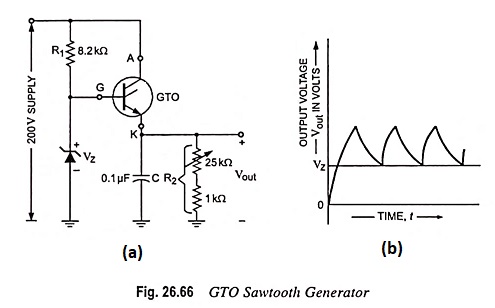
When the supply is switched on, the GTO will turn on, resulting in the short-circuit equivalent from anode to cathode. As a consequence the capacitor C will begin to charge toward the supply voltage, as illustrated in Fig. 26.66 (a). As the voltage across the capacitor C exceeds the zener potential, there will be a reversal in gate-to-cathode voltage resulting in a reversal of gate current. Eventually, the negative gate current will be large enough to turn the GTO off. Now the capacitor C will begin to discharge through resistor R2 because turning off of GTO results in the open-circuit equivalent from anode to cathode. The discharge time will be determined by the circuit time constant τ = CR2. The proper choice of R2 and C will result in the sawtooth waveform shown in Fig. 26.66 (b). Once the output voltage Vout drops below zener voltage Vz, the GTO will turn on and the process will repeat.