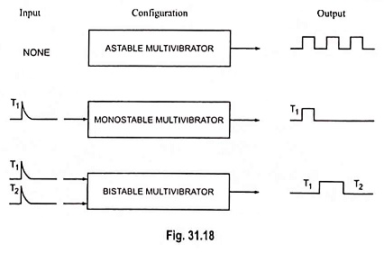
Astable Multivibrator Definition and its Working:
The multivibrator circuit which has no stable state is called the astable multivibrator. The two states of operation of astable multivibrators are quasi-stable (temporary) states. The astable multivibrator, therefore, makes successive transitions from one quasi-stable state to the other one after a predetermined time interval, without the help of an external triggering circuit. The periodic time depends upon the circuit time constants and parameters. The output of the circuit is a square wave with two time periods T1 and T2. If T1 = T2= T/2, the circuit is a symmetric astable multivibrator. If T1 # T2 it is called unsymmetric astable multivibrator. Since the output of an astable multivibrator oscillates in between off and on states freely, it is called a free-running multivibrator, The main application of an astable multivibrator is as a clock in digital circuits.
The astable multivibrator is essentially a square-wave generator. We consider three circuits: the collector-coupled astable multivibrator, the emitter-coupled astable multivibrator and complementary transistor astable multivibrator.
Collector Coupled Astable Multivibrator:
The circuit arrangement of Collector Coupled Astable Multivibrator is shown in Fig. 31.19. It is essentially a two-stage R-C coupled amplifier with the output of first stage coupled to the input of second stage; and the output of second stage coupled to the input of the first stage. As the phase of a signal is reversed when amplified by a single stage common emitter amplifier, it comes back to its original phase when passed through two stages. Thus, the signal fed back to the base of either transistor is in the same phase as the original signal at its output. It amounts to a positive feedback. The amount of feedback is so large that the transistors are driven between cut-off and saturation almost instantaneously. A transistor remains in either saturation or cut-off for a period depending on the time constant of the base-circuit elements.
Operation:
The operation of the Collector Coupled Astable Multivibrator circuit illustrated in Fig. 31.19 is as follows :
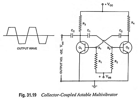
When power is first applied to the circuit, both transistors start conducting. Because of small differences in their operating characteristics, one of the transistors will conduct slightly more than the other. This starts a series of events. Assume arbitrarily that Q1 initially conducts more than Q2. This causes the collector voltage of Q1 to drop more rapidly than that of Q2. The resulting negative signal is fed to the base of Q2 through capacitor C1 and drives it towards cut-off. As a result the collector voltage of Q2 rises towards VCC.
This change in collector voltage of Q2 is fed to the base of Q1 through capacitor C2. It causes transistor Q1 to go into saturation. This happens so quickly that capacitor C1 does not get a chance to discharge, and the reduced voltage at the collector of Q1 appears across resistor R2.
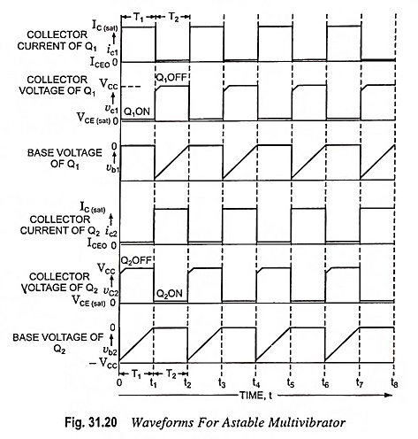
The switching action now begins, capacitor C1 begins to discharge exponentially through R2. When the voltage on C1 reaches zero volt, C1 attempts to charge up to the value of + VBB, the base supply voltage. But this action immediately places a forward bias on Q2 and thus transistor Q2 begins to conduct. As soon as Q2 starts conducting, its collector current causes collector voltage to fall. This negative-going voltage signal is fed to the base of transistor Q1 through capacitor C2 which begins to conduct less i.e., it comes out of saturation. This resulting increased voltage at the collector of Q1 is coupled through C1 and appears across R2. The collector current of Q2, therefore, increases. This process continues rapidly until transistor Q1 finally cuts off and transistor Q2 conducts heavily. At this instant, the collector voltage of transistor Q1 attains its maximum value of VCC, capacitor C1 charges to the full value of VCC, and a full cycle of operation has been completed. The cycle then repeats itself. The output of the multivibrator can be taken from the collector of either transistor. The output is a square wave, as shown in Fig. 31.20 and whose frequency is determined by R1, R2, C1 and C2 in the circuit.
Frequency of Oscillation:
From the above discussion it is found that as soon as astable multivibrator is switched on, transistor Q1 goes on while transistor Q2 goes off. Let this instant be t = 0.
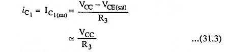
At time = 0 For Transistor Q1 (in On-state)
Collector voltage,
![]()
Collector current,
Base voltage,
![]()
Base current,
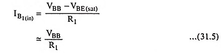
For Transistor Q2 (in off state)
Collector voltage,
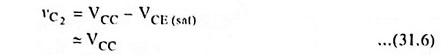
Collector current,
![]()
At the instant of switching on the power supply but before the commencement of regenerative feedback sequence, the voltage on capacitor C1 is VCC. This implies that the collector side voltage of the capacitor C1 is VCC and base side voltage is VB2(on). At the end of the regenerative cycle, the collector side voltage of the capacitor C1 has decreased from VCC to VCE (sat) (almost zero). But the capacitor C1 cannot discharge instantaneously. Thus the voltage at the base of the transistor Q2 is given as
![]()
After commencement of regenerative feedback but before Q1 goes off (i.e., 0 < t < T1), voltage across capacitor C1 increases from VB2(off) (t = 0) towards VBB. Charging path is provided by capacitor C1 and resistor R2 assuming that VC1 = 0. At any instant t, voltage VB2 is given as
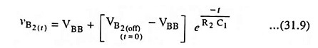
Thus, the base voltage of transistor Q2, VB2(t) rises exponentially with time constant C1R2. However, as soon as VB2 becomes equal to VB2(on) at time T1, the transistor Q2 commences conducting and VB2(t) remains constant at VB2(on) .
At time T1
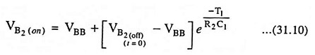
Solving Eqs. (27.8) and (27.10) we get
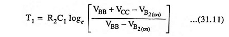
If VBB >> VB2(on), Eq. (31.11) becomes

and if VBB = VCC, then Eq. (31.12) reduces to
![]()
From Eq. (31.13) the on-time of transistor Q1 or the off-time of transistor Q2 is given as
![]()
Similarly, the off-time of transistor Q1 or the on-time of transistor Q2 is given as
![]()
Hence, total time period of square wave
![]()
For a symmetrical multivibrator R1 = R2 = R (say) and C1 = C2 = C (say) then total time period is given as
![]()
Frequency of the square wave,

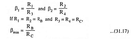
Minimum Values of β: For sustained oscillations, the transistors must saturate for which minimum values of β are as below
Emitter Coupled Astable Multivibrator:
In an Emitter Coupled Astable Multivibrator circuit capacitor C is connected between emitters of two transistors, as shown in Fig. 31.21. Transistor Q1 remains either in saturation or in cutoff while transistor Q2 is either in cut-off region or in active region. Capacitor C is a storage element. Let the transistor Q2 start conducting first.
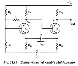
As soon as Q2 starts conducting, a current flows through RC2 making its collector voltage to fall and a voltage drop across RE2 too. This drop is followed by RE1 as voltage across capacitor C cannot change instantaneously. This emitter voltage keeps transistor Q1 off. Now the capacitor C begins charging in the direction shown in Fig. 31.21 and as a result emitter voltage of transistor Q1 starts falling.
When capacitor C charges to a level so that emitter voltage of transistor Q1 falls to a level to make it conducting. When transistor Q1 starts conducting, its collector voltage drops causing base voltage of transistor Q2 to fall. Thus transistor Q2 goes into cutoff region. Now capacitor C starts charging in reverse direction and when it goes to a level so that emitter voltage of transistor Q2 falls to force it to conduct. When transistor Q2 begins conducting and voltage drop across RE2 rises coupling to emitter of Q1. Thus Q1 is cutoff. Thus one cycle of operation is completed.
An emitter coupled astable multivibrator has the following advantages over a collector-coupled astable multivibrator.
- Collector of transistor Q2 is not connected to any part of the circuit, so it can be used to provide an output terminal.
- Frequency adjustment is easy because of use of only one capacitor in the circuit.
- Synchronization is easily possible at base of transistor Q1 as input at base is isolated.
- There are no recovery transients (such as overshoot voltages) in the output.
However, the emitter coupled astable multivibrator has the drawbacks of using more components and difficulty in obtaining proper operating conditions.
Complementary Transistor Astable Multivibrator:
An astable multivibrator can be realized by using a complementary pair of transistors. In the Complementary Transistor Astable Multivibrator both the transistors are either on or off simultaneously when switched on. This is contrary to two transistor astable multivibrator, where, at any instant of time, one of the transistor is on and the other is off, and these states change sequentially. The noteworthy point is that a complementary transistor astable multivibrator consumes very little power, since the power is drawn from the supply for a very short time duration when both the transistors are on simultaneously.
![]()
The circuit diagram of a complementary transistor astable multivibrator is shown in Fig. 31.23 (a). Here Q1 is PNP transistor and Q2 is NPN transistor.
Operation:
When the power supply is switched on at time t = 0, the voltage across capacitor, which was initially zero, rises exponentially towards VCC. When the instantaneous voltage across capacitor C attains the voltage level of (Vz + Vγ), the emitter-base junction of NPN transistor Q2 is at the edge of forward bias, Vz being zener voltage and Vγ is the cut-in voltage of the transistor.
Now when the NPN transistor Q2 starts conducting, its collector current flows via the emitter-base junction of PNP transistor Q1. Here the collector current of NPN transistor is the base current of PNP transistor. Further the collector current of PNP transistor is also in part of the base current of NPN transistor. Thus, any increase in base current of NPN transistor via the zener diode will abruptly bring both the transistors in saturation and the capacitor C is instantaneously discharged. As the capacitor C discharges, the base currents of both the transistors Q1 and Q2 are reduced and consequently both the transistors are off. Again the capacitor C starts charging and the process repeats itself. Resistance R2 limits the capacitor discharge current. If V1 is the residual voltage across the capacitor, when the switch is off, then the repetition period T is given by expression
![]()