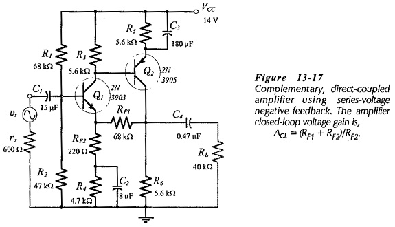
Two Stage Direct Coupled BJT Amplifier Circuit:
The Two Stage Direct Coupled BJT Amplifier Circuit in Fig. 13-17 is reproduced from Fig. 12-22, and modified to include feedback components RF1 and RF2. Other direct-coupled circuits can be converted into negative feedback amplifiers by following the same procedure. Similarly, BIFET circuits, both Two Stage Direct Coupled BJT Amplifier Circuit and capacitor-coupled, can be designed for overall negative feedback. As always, the best approach is to first design the circuit as a non-feedback amplifier, then determine the feedback component values.
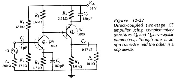
Note that there is no coupling-capacitor for the feedback network in the circuit shown in 13-17. This is because the omission of the capacitor can have a negligible effect on the circuit dc conditions if feedback resistor RF1 is large enough.
DC Feedback Pair Using Negative Feedback:
Figure 13-18(a) shows a dc feedback pair with ac feedback components CF1, RF1, and RF2. This is the most economical of all two-stage BJT amplifier circuits, because it has the smallest quantity of components. It can have just as high a voltage gain (open-loop and closed-loop) as any other two-stage circuit. As a negative feedback amplifier, its input resistance is normally higher than that for a BJT circuit using voltage divider bias, (R2 is usually larger than the parallel resistance of voltage divider resistors). As always, the feedback components are determined after the circuit is designed for the largest possible open-loop voltage gain.
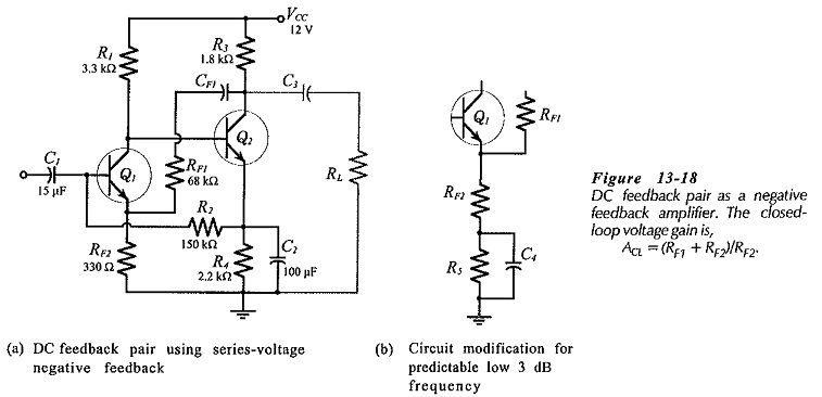
The lower cutoff frequency for the circuit in Fig. 13-18(a) is unpredictable. The modification shown in Fig. 13-18(b) gives a definite low 3 dB frequency, (when XC4 = RF2). In this case, emitter resistor R5 affects the circuit dc bias conditions, so it must be designed into the circuit from the start. As in other circuits, it might be possible to omit the feedback network coupling capacitor, (CF1 in Fig. 13-18). The direct current through RF1 should be calculated to ensure that it does not significantly affect the bias conditions of the circuit.
BIFET Two-Stage Circuit With Negative Feedback:
A two-stage, direct-coupled, BIFET circuit with series-voltage negative feedback is shown in Fig. 13-19.
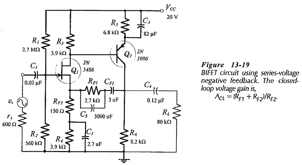
The open-loop voltage gain of a BIFET circuit is typically 50 to 100 times smaller than that for a two-stage BJT amplifier. Therefore, BIFET negative feedback amplifiers must be designed for relative small closed-loop voltage gains, usually a maximum of around 30. The single major advantage of BIFET circuits, very high input impedance, is largely unchanged by negative feedback. The design procedure for the feedback network in the BIFET circuit is exactly as already discussed.
Setting the Circuit Upper Cutoff Frequency:
The upper cutoff frequency of any of the series voltage negative feedback amplifiers already discussed can be set by the simple process of connecting a capacitor (CS) across feedback resistor RF1, as illustrated in Fig. 13-19. It can be shown that f2 occurs when XCS = RF1, so long as the upper cutoff frequency without CS is much higher than the desired f2 value. Therefore, to determine CS
![]()