Two Stage Differential Amplifier with Negative Feedback:
The circuit shown in Fig. 13-20 has a Two Stage Differential Amplifier with Negative Feedback with npn BJTs, and a direct-coupled pnp transistor differential amplifier second stage. The circuit uses a plus/minus supply voltage, and the base terminals of Q1 and Q2 are biased to ground via resistors R1 and R6, respectively. Transistors Q3 and Q4 have the bases directly connected to the collector terminals of Q1 and Q2. So, bias voltage for Q3 and Q4 bases is provided by the voltage drops across the Q1 and Q2 collector resistors, (R2 and R4).
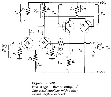
The amplifier input terminal is the base of Q1, and the output is taken from Q3 collector. No collector resistor is provided for Q4, because no output or feedback is taken from Q4. Note that the feedback network (R5 and R6) is connected from the output at the collector of Q3 back to the base of Q2. Because the emitter of Q2 is directly coupled to Q1 emitter, applying the feedback voltage (vf) to Q2 base is similar to applying it to Q1 emitter.
DC Bias Conditions:
The circuit in Fig. 13-20 is designed to have the do bias voltage at Q2 base equal to Q1 base bias voltage; in this case, ground level. This means that the do voltage at the collector of Q3 must also equal the Q1 base voltage, because Q3 collector is directly connected to Q2 base via R5. Consider what would happen if VC3 (at the output terminal ) is not exactly equal to VB1 (at the input).
Suppose VC3 goes lower than its normal level:
- VB2 is reduced below the level of VB1, and this reduces IC2 and increases IC1.
- The increased level of IC1 causes an increased voltage drop across R2, and the reduced level of IC2 decreases the voltage drop across R4. Thus VB3 is increased and VB4 is decreased.
- This raises the level of IC3 and lowers IC4. So, VRB is increased (by the IC3 increase) to drive VC3 back up to its normal voltage. Similarly, if VC3 somehow drifts to a higher than normal level:
- VB2 is raised above the level of VB1, thus increasing IC2 and reducing IC1.
- The decreased level of IC1 and increased level of IC2 produces voltage drops across R2 and R4 that reduce VB3 and increase VB4.
- This change reduces IC3, thus decreasing VRB to drive VC3 back down to its normal voltage.
It is seen that there is do negative feedback that stabilizes the circuit bias conditions.
AC Operation:
Consider the circuit waveforms shown in Fig. 13-21. A positive-going input signal (vi) at the base of Q1 produces a positive-going output (vo) at Q3 collector. As in the case of the dc bias conditions, the instantaneous ac voltage at Q2 base follows the instantaneous level of the ac signal voltage at Q1 base.
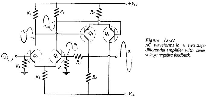
With vb2 = vb1, or vi = vf,
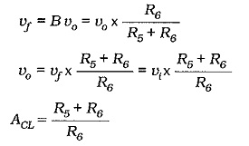
Resistors R5 and R6 in Figs. 13-20 and 13-21 are comparable to RF1 and RF2, respectively, in the other negative feedback circuits already discussed. So, the closed-loop gain equation is the same equation that applies in the case of all series-voltage negative feedback amplifiers. As always, the equation is true only when the open-loop gain is very much larger than the closed-loop gain.
The input and output impedances for a circuit with a Two Stage Differential Amplifier with Negative Feedback are calculated exactly as discussed for other negative feedback circuits.
Note that there are no bypass capacitors in the circuit in Figs. 13-20 and 13-21. If the signal and load are capacitor coupled to the circuit, the coupling capacitors determine the lower cutoff frequency. If the signal and load are direct coupled, then the circuit is a dc amplifier; one that amplifies direct voltage signals.
Circuit Design:
The second stage components are determined in essentially the same way as the input stage components, bearing in mind that the second stage is upside down compared to the input stage. Feedback network resistor R6 at the base of Q2 is selected equal to bias resistor R1 at Q1 base. This is to equalize the resistances at the bases of Q1 and Q2, and thus equalize any voltage drops due to IB1 and IB2. R5 is calculated from the specified closed loop gain and the R6 resistance.
Modification for Reduced Zout:
Although the application of series-voltage negative feedback substantially reduces the output impedance of a circuit, further reduction of Zout is sometimes required. Figure 13-23 shows the circuit of Fig. 13-22 with the addition of an emitter follower output stage (Q5). Note that the feedback network is now connected at the emitter follower output terminal.
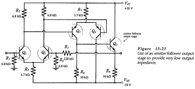
The output impedance at Q5 emitter terminal in Fig. 13-23 is found from the common-collector circuit
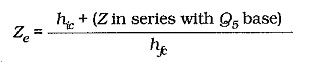
This gives,
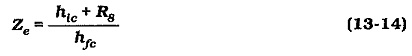
This quantity is modified by negative feedback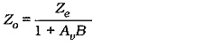
Then, as always, the circuit output impedance which must also be rewritten for the circuit in Fig. 13-23.
![]()
An emitter follower output stage can be added to any of the amplifiers previously discussed. However, the combination of an emitter follower output stage with a differential amplifier has a particular significance.