Two Diode Full Wave Rectifier Circuit:
The Fig. 3-2 shows the Two Diode Full Wave Rectifier Circuit, and its input voltage is supplied from a transformer (T1) with a center-tapped secondary winding. The circuit is essentially a combination of two half-wave rectifier circuits, each supplied from half of the transformer secondary.
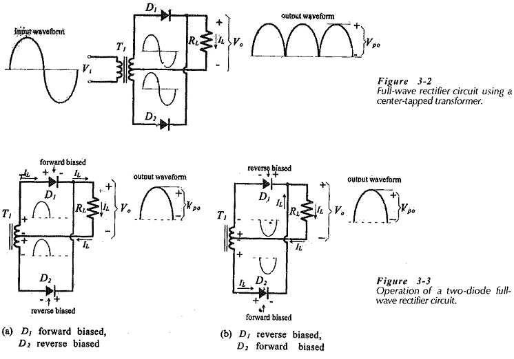
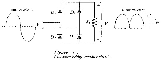
When the transformer output voltage is positive at the top, as illustrated in Fig. 3-3(a), the anode of D1 is positive, and the center-tap of the transformer is connected to the cathode of D1 via RL. Consequently, D1 is forward biased, and load current (IL) flows from the top of the transformer secondary through D1, through RL from top to bottom, and back to the transformer center-tap. During this time, the polarity of the voltage from the bottom half of the transformer secondary causes diode D2 to be reverse biased.
For the duration of the negative half-cycle of the transformer output, the polarity of the transformer secondary voltage causes D1 to be reverse biased and D2 to be forward biased, [see Fig. 3-3(b)]. IL flows from the bottom terminal of the transformer secondary through diode D2, through RL from top to bottom, and back to the transformer center-tap. The output waveform is the combination of the two half-cycles; that is, a continuous series of positive half-cycles of sinusoidal waveform. This is Two Diode Full Wave Rectifier Circuit rectification.
Bridge Rectifier:
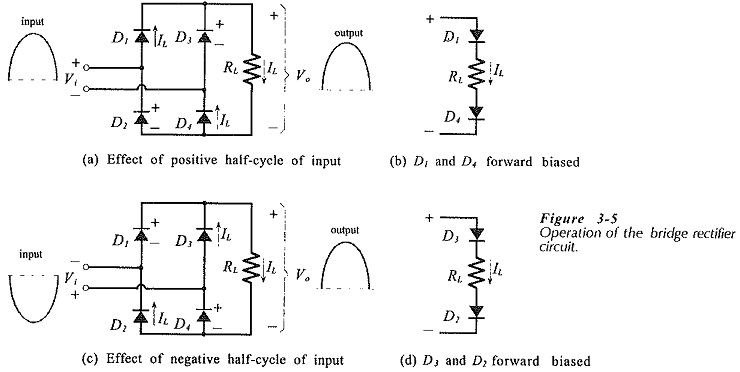
The center-tapped transformer used in the circuit of Fig. 3-2 is usually more expensive and requires more space than additional diodes. So, a bridge rectifier is the circuit most frequently used for full-wave rectification.
The bridge rectifier circuit in Fig. 3-4 is seen to consist of four diodes connected with their arrowhead symbols all pointing toward the positive output terminal of the circuit. Diodes D1 and D2 are series-connected, as are D3 and D4. The ac input terminals are the junction of D1 and D2 and the junction of D3 and D4. The positive output terminal is at the cathodes of D1 and D3, and the negative output is at the anodes of D2 and D4.
During the positive half-cycle of input voltage, diodes D1 and D4 are in series with RL, as illustrated in Figs. 3-5(a) and (b). Thus, load current (IL) flows from the positive input terminal through D1 to RL, and then through RL and D4 back to the negative input terminal. Note that the direction of the load current through RL is from top to bottom. During this time, the positive input terminal is applied to the cathode of D2 and the negative output is at D2 anode, [see Fig. 3-5(a)]. So, D2 is reverse biased during the positive half-cycle of the input. Similarly, D3 has the negative input at its anode and the positive output at its cathode during the positive input half-cycle, causing D3 to be reverse biased.
Figures 3-5(c) and (d) show that diodes D2 and D3 are forward biased during the negative half-cycle of the input waveform, while D1 and D4 are reverse biased. Although the circuit input terminal polarity is reversed, IL again flows through RL from top to bottom, via D3 and D2.
It is seen that during both half-cycles of the input, the output terminal polarity is always positive at the top of RL, negative at the bottom. Both positive and negative half-cycles of the input are passed to the output. The negative half-cycles are inverted, so that the output is a continuous series of positive half-cycles of sinusoidal voltage.
The bridge rectifier has two forward-biased diodes in series With the supply voltage and the load. Because each diode has a forward voltage drop (VF), the peak output voltage is,
![]()
As in the case of the half-wave rectifier, a reservoir capacitor substantially changes the full-wave rectified output voltage waveform and affects the diode current and voltage requirements.
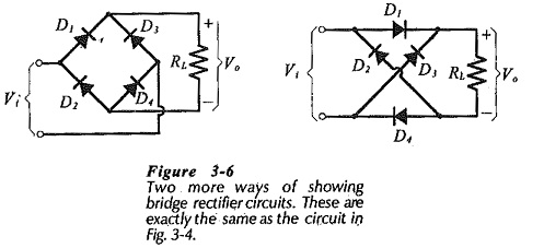
Figure 3-6 shows two common methods of drawing a bridge rectifier circuit. Although they both look more complex than the circuit in Fig. 3-4, comparison shows that they are exactly the same circuit. The cathodes of D1 and D3 in all three circuits are connected to the positive output terminal, and the anodes of D2 and D4 are connected to the negative output terminal. Also, the ac input is applied to the junction of D1 and D2 and the junction of D3 and D4.