Transistor Fabrication Techniques:
Different Transistor Fabrication Techniques are namely
- Alloy Transistor
- Micro Alloy Transistor
- Microalloy Diffused Transistor
- Diffuse Mesa Transistor
- Epitaxial Mesa Transistors
- Diffused Planar Transistor
- Annular Transistor
1. Alloy Transistor:
For manufacture of alloy Transistor Fabrication Techniques, single-crystal n-type wafers are scribed into many small sections, or dice, each of which forms the substrate for one transistor. A small pellet of p-type material is melted on one surface of each section until it partially penetrates and forms an alloy with the substrate, [Fig. 7-10(a)], thus creating a pn-junction. The process is repeated on the other side of the wafer to constitute a pnp transistor.
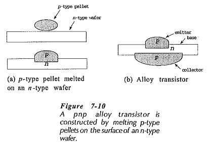
One of the junctions has a large area and one has a small area, as illustrated in Fig. 7-10(b). The small-area junction becomes the emitter base junction, and the larger one becomes the collector-base junction. One reason for this is that the large area junction most easily collects all of the charge carriers emitted from the small-area junction. Another more important reason is that most of the power is dissipated at the transistor collector-base junction.
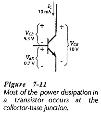
Suppose a silicon transistor has IC = 10 mA and VCE = 10 V, (see Fig. 7-11). The total power dissipate in the transistor is,
![]()
The base-emitter voltage is VBE = 0.7 V, and the collector-base voltage is,
![]()
The power dissipated at the base emitter junction is,
![]()
and, the power dissipated at the collector base junction is,
![]()
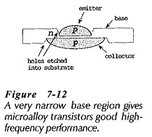
2. Micro Alloy Transistor:
Because very narrow base widths are difficult to obtain with alloy transistors, they are not suitable for high frequency applications. To improve the high-frequency performance, holes are first etched into the wafer from each side, leaving a very thin layer, (Fig 7-12). By a plating process, surfaces of impurity material are formed on each side of the thin n-type portion. Heat is then applied to alloy the impurities into the base region. This process produces very thin base regions and good high-frequency performance. The device is termed a micro alloy transistor.
3. Microalloy Diffused Transistor:
In microalloy Transistor Fabrication Techniques, the collector-base depletion region penetrates deeply into the very thin base. Thus, a major disadvantage is that punch-through can occur at very low collector voltages. Microalloy diffused transistors use a substrate that is initially undoped. After the holes are etched into each side of the wafer to produce the thin base region, the base is doped by diffusion from the collector side. The diffusion can be carefully controlled so that the base region is heavily doped at the collector side, with the doping becoming progressively less until the material is almost intrinsic (undoped) at the emitter. With this kind of doping, the collector-base depletion region penetrates only a short distance into the base, so that high punch-through voltages are achieved.
4. Diffuse Mesa Transistor:
In the production of mesa Transistor Fabrication Techniques, several thousand transistors are simultaneously formed on the wafer, by the diffusion process. As shown in Fig. 7-13, the main body of the wafer becomes the n-type collectors, the diffused p-regions become the bases, and the final n-regions are the emitters. Metal films are deposited on the base and emitter surfaces for contacts.
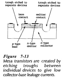
The transistors could be separated by the usual process of scribing lines on the surface of the wafer and breaking it into individual units. However, this produces very rough edges that result in relatively high leakage currents between collector and base. So, before cutting the wafer, the transistors are isolated by etching away the unwanted portions of the diffused area to form troughs between devices. As illustrated, the base and emitter regions now project above the main wafer which forms the collector region. This is the mesa structure, The narrow base widths that can be achieved by the diffusion process make the mesa transistor useful at very high frequencies.
5. Epitaxial Mesa Transistors:
One of the disadvantages of the process just described is that, because the collector region is highly resistive, diffused mesa transistors have a high saturation voltage. Such devices are unsuitable for saturated switching applications. This same characteristic (high collector resistance) is desirable for high punch-through voltage. One method of achieving both high punch-through voltage and low saturation level uses the epitaxial process, to produce an epitaxial mesa Transistor Fabrication Techniques.
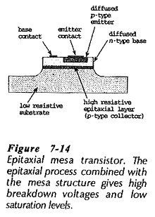
Starting with a low-resistive (highly doped) wafer, a thin, highly resistive epitaxial layer is grown. This layer becomes the collector, and the base and emitter are diffused as already discussed. The arrangement is illustrated in Fig. 7-14. The punch-through voltage is high because the collector-base depletion region spreads deepest into the lightly doped collector. Saturation voltage is low, because the collector region is very narrow and the main body of the wafer through which collector current must flow has a very low resistance.
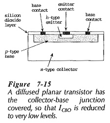
6. Diffused Planar Transistor:
In all the previously described Transistor Fabrication Techniques the collector-base junction is exposed (within the transistor package), and substantial charge carrier leakage can occur at the junction surface. In the diffused planar transistor illustrated in Fig. 7-15, the collector-base junction is covered with a layer of silicon dioxide. This construction gives a very low collector-base leakage current (ICBO); typically 0.1 nA.
7. Annular Transistor:
A problem which occurs particularly with pup planar transistors is the induced channel. This results when a relatively high voltage is applied to the silicon dioxide surface, (at one of the terminals). Consider the pup structure shown in Fig. 7-16(a). If the surface of the silicon dioxide has a positive voltage, minority charge carriers within the lightly doped p-type substrate are attracted by the positive potential. The minority charge carriers concentrate at the upper edge of the substrate and form an n-type channel from the base to the edge of the device. This becomes an extension of the n-type base region and results in charge carrier leakage at the exposed edge of the collector-base junction.
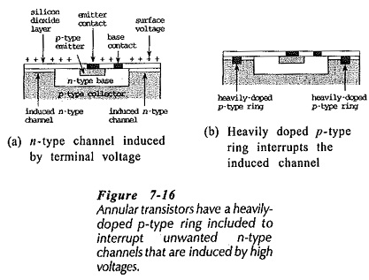
The problem arises because the p-type substrate is highly resistive. If it were heavily doped with p-type charge carriers, the concentration of n-type carriers would be absorbed (the electrons would be swallowed by holes). The introduction of a heavily doped p-type ring around the base, as in Fig. 7-16(b), interrupts the induced channel and isolates the collector-base junction from the device surface. The annular transistor, therefore, is a high-voltage device with the low collector-base leakage of the planar transistor.