Transistor Datasheet:
To select a transistor for a particular application, the Transistor Datasheet provided by device manufacturers must be consulted.
Most data sheets start off with the device type number at the top of the page, a descriptive title, and a list of major applications for the device. This information is usually followed by mechanical data in the form of an illustration showing the package shape and dimensions, as well as indicating which leads are collector, base, and emitter, (see Fig. 8-1).
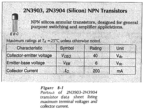
The absolute maximum ratings of the transistor at a temperature of 25°C are listed next. These are the maximum voltages, currents, and power dissipation that the device can survive without breaking down. It is very important that these ratings never be exceeded; otherwise, failure of the device is quite possible. For reliability, the maximum ratings should not even be approached. The maximum transistor ratings must also be adjusted downward for operation at temperatures greater than 25 °C.
Following the absolute maximum ratings, the Transistor Datasheet normally shows a complete list of electrical characteristics for the device. Again, these are specified at 25°C, and allowances are necessary for temperature variations.
A complete understanding of all the quantities specified on a Transistor Datasheet will not be achieved until circuit analysis and design is studied. Some of the most important quantities are considered below. It is important to note that the ratings for a given transistor are stated for specified circuit conditions. The ratings are no longer valid if these conditions change.
VCBO : Collector-base voltage — maximum dc voltage for reverse-biased collector-base junction.
VCEO : Collector-emitter voltage — maximum collector-emitter dc voltage with base open-circuited.
VEBO : Emitter-base voltage — maximum emitter-base reverse-bias dc voltage.
IC : Collector current — maximum dc collector current.
ICBO or ICO : Collector cutoff current — dc collector current with the collector-base junction reverse biased and the emitter open-circuited.
VCE(sat) : Collector-emitter saturation voltage — collector-emitter voltage with the device in saturation.
hFE : Static forward current transfer ratio — common emitter ratio of dc collector current and base current.
NF : Noise figure — ratio of total noise output to total noise input expressed as a decibel (dB) ratio. Defines the amount of noise added by the device.
fhfe or fαe : Common emitter cutoff frequency — common emitter operating frequency at which the device current gain falls to 0.707 of its normal (mid-frequency) value.
fhfb or fαb : Common base cutoff frequency — as above, for common base.
From the section of the 2N3903-2N3904 data sheet reproduced in Fig. 8-1, the maximum collector-emitter voltage is specified as VCEO = 40 V. Obviously, this device should not be used in any circuit with a supply exceeding 40 V; otherwise the transistor might break town. Preferably, the circuit supply voltage should always be less than the specified maximum VCEO.
The maximum VEB is listed as 6 V. This is the highest voltage that may be applied in reverse across the base-emitter junction of the transistor. If a greater voltage is used, the base-emitter junction of the transistor is likely to break down. The maximum (reverse) VEB for most transistors is 5 V. In circumstances where the applied voltage might exceed this level, a clipping circuit may be used. Alternatively, a diode can be connected in series with the transistor emitter to increase the breakdown voltage, as shown in Fig. 8-2. The normal forward biased base-emitter voltage for a transistor is, of course, approximately 0.7 V for a silicon transistor and approximately 0.3 V for a germanium transistor.
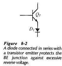
Figure 8-3 shows sections of a transistor data sheet which specify the dc current gain hFE, and the small signal (or ac) current gain hfe. For a 2N3904 device with IC = 10 mA, hFE is listed as 100 minimum and 300 maximum, (see the solid underlined quantities). If the transistor collector current is to be around 1 mA, then the minimum hFE is 70, (dashed underlined). The maximum hFE for IC = 1 mA is not specified. It is unlikely that hFE(max) would exceed 300 for this condition. However, because the manufacturer does not list a maximum value, it remains uncertain. This situation illustrates the importance of reliable bias circuits that make IC and VCE largely independent of hFE.
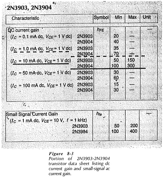
The small-signal current gain (hfe) for a 2N3904 is listed in Fig. 8-3 as 100 minimum and 400 maximum. Once again, this parameter is specified for a particular set of bias conditions. The signal frequency at which hfe was measured is specified as 1 kHz. Section 8-2 discusses the fact that hfe decreases at high frequencies.