Transistor Circuit Noise:
Unwanted signals at the output of an electronics system are termed noise. The noise amplitude may be large enough to severely distort, or completely swamp, the wanted signals. Consequently, the noise level dictates the minimum signal amplitude that can be handled. Noise originates as atmospheric noise from outside the system and as Transistor Circuit Noise generated within resistors and devices.
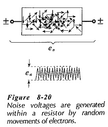
Consider a conductive material at room temperature, (Fig. 8-20). The motion of free electrons drifting around within the material constitutes a flow of many tiny random electric currents. These currents cause minute voltage drops, which appear across the ends (or terminals) of the material. Because the number of free electrons available and the random motion of the electrons are both increased as temperature rises, the generated voltage amplitude is proportional to temperature. This unwanted, randomly varying voltage is termed thermal noise.
Thermal noise is generated within resistors, and when the resistors are at the input stage of an amplifier, the noise is amplified and produced as an output. Noise from other resistors is not amplified as much as that from the resistors right at the input; consequently, only the input stage resistors need be considered in noise calculations. Noise is also generated within a transistor, and like resistors, the input stage transistor is the most important because its noise is amplified more than that from any other stage.
Because thermal noise is an alternating quantity, its rms output level from any amplifier is dependent upon the bandwidth of the amplifier. It can be shown that the rms noise voltage generated in a resistance is,
![]()
where,
k = Boltzmann’s constant= 1.374 x 10⁻²³ J/K (i.e., joules per degree Kelvin)
T= absolute temperature (Kelvin)
R = resistance in ohms
B = circuit bandwidth
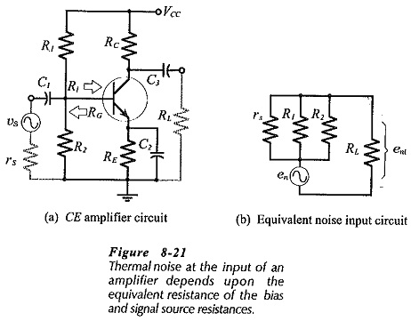
In the circuit shown in Fig. 8-21(a) R1 and R2 are bias resistors; es is a signal voltage with source resistance rs. The total noise-generating resistance (RG) in parallel with the amplifier input terminal is
![]()
In the noise equivalent circuit [Fig. 8-21(b)] , en is the noise voltage generated by RG. If the device input resistance is Ri, then the noise voltage is divided,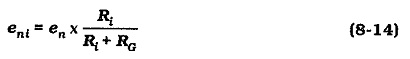
If the amplifier voltage gain is Av, the output noise due to RG is
![]()
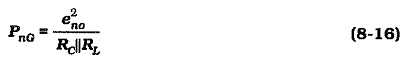
With a circuit collector resistance RC and load resistance RL, the noise output power produced by RG is,
To specify the amount of noise generated by a transistor, manufacturers usually quote a noise figure (NF). To arrive at this figure, the transistor noise output is measured under specified bias conditions and with a specified source resistance, temperature, and noise bandwidth. The noise figure defines the amount of noise added by the transistor to the noise generated by the specified resistance (RG) at the input. Recall that RG is the combined bias and signal source resistances, as seen from the amplifier input.
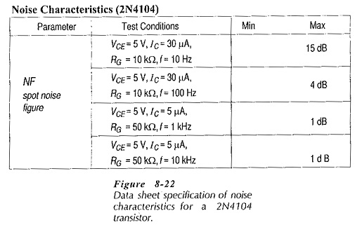
The data sheet portion in Fig. 8-22 specifies spot noise figures for a 2N4104 transistor. This means that the noise has been measured for a bandwidth of 1 Hz. The bias conditions are listed because the transistor noise can be affected by VCE and IC. Note that the specified IC levels are very low (5 μA to 30 μA), because transistor noise increases with increasing current levels.
The noise factor (F) is the total Transistor Circuit Noise power output divided by noise output power from the source resistor.
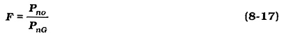
The noise figure (NF) is the decibel value of F,
![]()
Ideally, a transistor would add no noise to the circuit, and its noise figure would be zero. Obviously, the smallest possible transistor noise figure is the most desirable.
If the circuit in which the transistor is employed does not have the value of source resistance and the bias conditions specified, then the specified noise figure does not apply. In this case the noise figures can still be used to compare transistors, but for accurate estimations of noise, a new measurement of the noise figure must be made. From Eq. 8-17, the total noise output power due to RG and the input transistor is,
![]()