Schmitt Trigger Circuit Diagram:
Inverting Schmitt Trigger – A Schmitt Trigger Circuit Diagram is a fast-operating voltage level detector. When the input voltage arrives at a level determined by the circuit components, the output voltage switches rapidly between its maximum positive level and its maximum negative level.
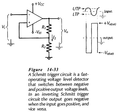
An op-amp inverting Schmitt Trigger Circuit Diagram is shown in Fig. 14-33 together with input and output waveforms. At first glance the circuit looks like a noninverting amplifier. But note that (unlike a noninverting amplifier) the input voltage (Vi) is applied to the inverting input terminal, and the feedback voltage goes to the noninverting input. The waveforms show that the output switches rapidly from the positive saturation (+Vo(sat)) voltage to the negative saturation level (-Vo(sat)) when the input exceeds a certain positive level; the upper trigger point (UTP). Similarly, the output voltage switches from low to high when the input goes below a negative triggering point; the lower trigger point (LTP).
Note that after Vi has increased to the UTP and Vo has switched to -Vo(sat), the output remains at -Vo(sat) even when Vi falls below the UTP. Switch over from -Vo(sat) to +Vo(sat) does not occur until Vi = LTP. Similarly, after Vi has been reduced to the LTP and Vo has switched to +Vo(sat), the output remains at +Vo(sat) when Vi is increased above the LTP. Switch-over from +Vo(sat) to -Vo(sat) does not occur again until Vi = UTP.
Triggering Points:
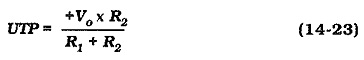
If the output voltage to the circuit in Fig. 14-33 Is high, the voltage at the noninverting terminal is,
If the input voltage (at the inverting input terminal) is below VR2 (at the noninverting input), the output voltage is kept at its high positive level. For the output to switch to its low level, the input voltage must exceed VR2 by a very small amount (approximately 70 μV for a 741 op-amp). So, the UTP essentially equals VR2.
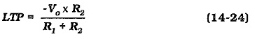
When the output is negative, the LTP can be calculated as,
Input/Output Characteristic:
A graph of output voltage (Vo) versus input voltage (Vi) can be plotted for an inverting Schmitt Trigger Circuit Diagram, as shown in Fig. 14-34. This is the circuit input/output characteristic.
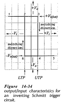
To understand the characteristic, consider the voltages at each of the numbered points on the graph:
- At point 1, Vo = +Vo(sat), and Vi < LTP, thus keeping Vo = +Vo(sat).
- From point 1 through points 2 and 3, Vo remains at +Vo(sat) as Vi is increased through the LTP and through zero, until Vi = UTP.
- From point 3 to point 4, Vo switches rapidly from +Vo(sat) to -Vo(sat) when Vi = UTP.
- From point 4 to point 5, Vo remains at -Vo(sat) as Vi is increased above the UTP.
- From point 5 through points 4 and 6, Vo remains at -Vo(sat) as Vi is reduced through the UTP and through zero, until Vi = LTP.
- From point 6 to point 2, Vo switches rapidly from -Vo(sat) to +Vo(sat) when Vi = LTP.
- From point 2 to point 1, Vo remains at +Vo(sat) as Vi is reduced below the LTP.
The difference between the UTP and the LTP is termed hysteresis. Some applications require a small amount of hysteresis, and for other applications a large amount of hysteresis is essential.
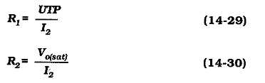
Circuit Design:
Design procedure for a Schmitt Trigger Circuit Diagram is similar to op-amp amplifier design. A voltage divider current (I2 in Fig. 14-33) is selected much larger than the op-amp input bias current. The resistor values are then calculated as,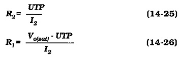
Adjusting the Trigger Points:
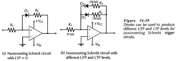
Many Schmitt trigger circuit applications require UTP and LTP levels that are not equal in magnitude. This is usually achieved by the use of diodes, as illustrated in Fig. 14-36.
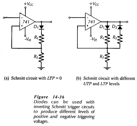
The circuit shown in Fig. 14-36(a) simply has a diode (D1) connected in series with resistor R1. The diode is forward biased only when the op-amp output is a positive quantity. At this time, the UTP is VR2, as before. When Vo is negative, D1 is reverse biased, making I2 equal zero. Consequently, there is no voltage drop across R2, and so the noninverting terminal is grounded via R2. This gives a zero level for the LTP. Thus, this circuit has a positive UTP and a zero voltage LTP.
Figure 14-36(b) shows a circuit with two different-level trigger points. When Vo is positive, D1 is forward biased and D2 is reversed, and the UTP is set by resistors R1 and R2. With Vo negative, D2 is forward biased and D1 is reversed. The LTP is now determined by the resistances of R3 and R2.
The diode forward voltage drop (VF) must be accounted for when calculating the trigger points for both of the circuits in Fig. 14-36. This is done simply by replacing Vo with (Vo(sat) – VF) in Eqs. 14-25 and 14-26. Another important design consideration is that the voltage divider current (I2) should normally be a minimum of 100 μA for satisfactory diode operation.
Noninverting Schmitt Trigger:
A noninverting Schmitt Trigger Circuit Diagram is shown in Fig. 14-37. This circuit looks like an inverting amplifier, but note that (unlike an inverting amplifier) the inverting input is grounded and the noninverting input is connected to the junction of R1 and R2. The waveforms in Fig. 14-37 show that Vo switches rapidly from -Vo(sat) to +Vo(sat) when Vi arrives at the UTP, and that Vo switches back to -Vo(sat) when Vi falls to the LTP.
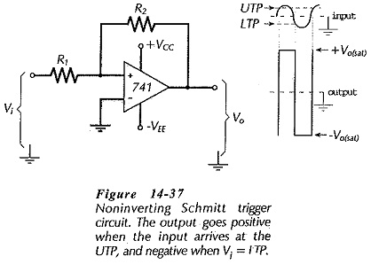
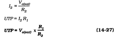
Consider the situation when Vi = UTP and Vo has just switched to +Vo(sat). The voltage at the junction of R1 and R2 is pulled up far above the ground level voltage at the op-amp inverting input terminal. So, the positive voltage at the noninverting input keeps the output at its positive saturation level. To switch the output to -Vo(sat), the voltage at the junction of R1 and R2 must be pulled down to the (ground level) voltage at the inverting input terminal. This occurs when Vi is at the LTP, [see Fig. 14-38(a)]. So, switching occurs when one end of R1 (the right end) is at ground, and the other (left) end is at Vi = LTP; that is, when VR1 = LTP. Similarly, switching in the other direction occurs when VR1 = UTP, [Fig. 14- 38(b)]. So, at the trigger points,
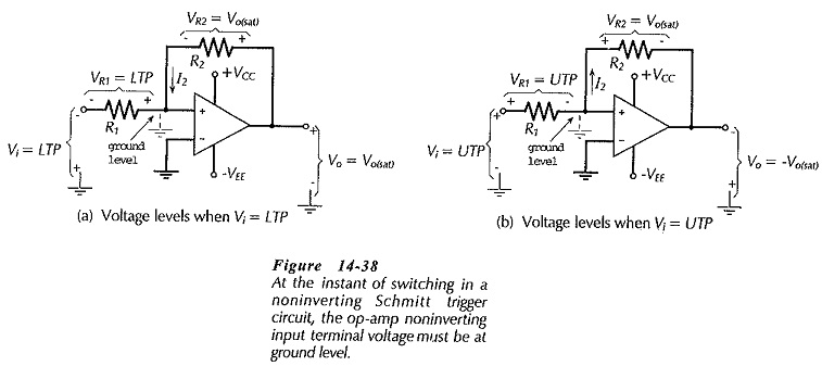
![]()
Figure 14-38(a) and (b) show that the output voltage is at one of its saturation levels at the instant of triggering. This means that one end of R2 is at ground (left end), and the other (right) end is at Vo(sat). So, VR2= Vo(sat) when triggering occurs.
Design procedure for a noninverting Schmitt Trigger Circuit Diagram is just as simple as for the inverting circuit. Voltage divider current I2 is again selected much larger than the op-amp input bias current.
Then the resistor values are,
Noninverting Schmitt trigger circuits can be designed for different upper and lower trigger point voltages by the use of diodes, as in the case of the inverting circuit. Figure 14-39(a) and (b) shows two possible circuits. The diode forward voltage drop (VF) must be included in the UTP and LTP calculations.