Power Dissipation Rating in Transistor:
Maximum Power Dissipation – Consider the portion of the data sheet for the 2N3903 and 2N3904 transistor reproduced in Fig. 8-24. The total device dissipation (PD) is specified as 625 mW at a maximum ambient temperature (TA) of 25°C. This means that (VCE x IC) must not exceed 625 mW when the surrounding air temperature is 25°C. Figure 8-1 lists the maximum IC and VCE for the 2N3903 and 2N3904 as 40 V and 200 mA, respectively. If these two quantities exist simultaneously at the transistor, the Power Dissipation Rating in Transistor is,
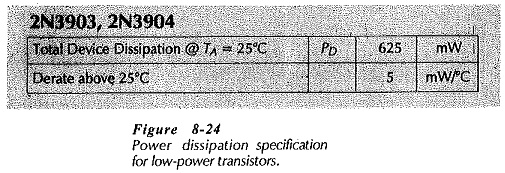
which is much greater than the 625 mW specified maximum.
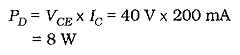
If the maximum VCE is used with a 2N3904 transistor, then the maximum collector current must not exceed,
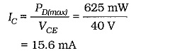
When the transistor has to pass the maximum IC, the VCE should be limited to,
If the air temperature is greater than 25°C, the Power Dissipation Rating in Transistor must be derated. From Fig. 8-24, the power derating factor for 2N3903-2N3904 transistors is 5 mW/°C. This may be used to calculate the device maximum power dissipation at any air temperature.
![]()
where D is the power dissipation derating factor.
The data sheet portion in Fig. 8-25 shows the voltage, current and-power ratings for a 2N3055 high-power transistor. The maximum dissipation is specified as 115 W at a case temperature (TC) of 25°C. Note that for a power transistor the case temperature is specified, instead of the air temperature. The derating factor is 0.667 W/°C.
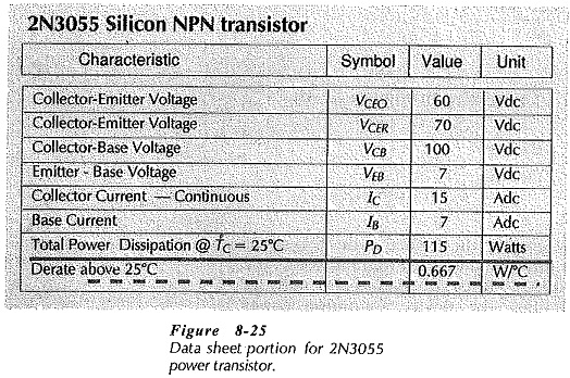
The maximum power dissipation at any temperature may be calculated for the 2N3055 by use of Eq. 8-20. Alternatively, a power Berating graph can be constructed for reading the device maximum power dissipation at any temperature.
Maximum Power Dissipation Curve:
When the maximum power that may be dissipated in a transistor is determined, the maximum IC level may be calculated for any given VCE, or vice versa. The corresponding voltage and current levels may be more easily determined by drawing a maximum power dissipation curve on the transistor output characteristics. To draw this curve, the greatest power that may ‘be dissipated at the operating temperature is first calculated. Then, using convenient collector-emitter voltage levels, the corresponding collector current levels are calculated for the maximum power dissipation. Using these current and voltage levels the curve is plotted on the device characteristics.
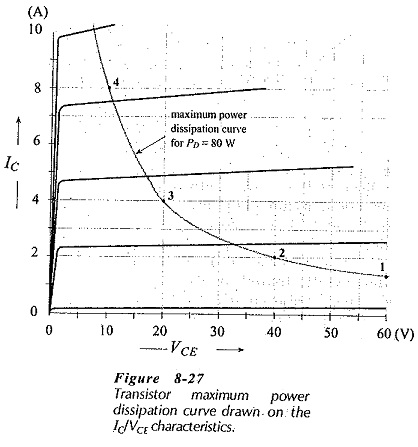
The transistor voltage and current conditions must at all times be maintained in the portion of the characteristics below the maximum power-dissipation curve. This means, for example, that all point on load lines must be below the curve.