RC Phase Shift Oscillator Circuit Diagram:
Figure 16-1 shows the RC Phase Shift Oscillator Circuit Diagram, which consists of an inverting amplifier and an RC phase-shifting network. The amplifier phase-shifts its input by -180°, and the RC phase-lead network phase-shifts the amplifier output by a +180°, giving a total loop phase shift of zero. The attenuated feedback signal (at the amplifier input) is amplified to reproduce the output. In this condition the circuit is generating its own input signal, consequently, it is oscillating. The output and feedback voltage wave forms in Fig. 16-1 illustrate the circuit operation.

For a state of oscillation to be sustained in any sinusoidal oscillator circuit, certain conditions, known as the Barkhausen criteria, must be fulfilled:
- The loop gain must be equal to (or greater than) one.
- The loop phase shift must be zero.
The RC phase-lead network in Fig. 16-1 consists of three equal-value resistors and three equal-value capacitors. Resistor R1 functions as the last resistor in the RC network and as the amplifier input resistor. A phase-lag network would give a total loop phase shift of -360°, and so it would work just as well as the phase lead network.
The frequency of the oscillator output depends upon the component values in the RC network. The circuit can be analysed to show that the RC Phase Shift Oscillator Circuit Diagram is 180° when
![]()
This gives an oscillation frequency,

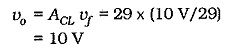
As well as phase shifting the amplifier output, the RC network attenuates the output. It can be shown that, when the required 180° phase shift is produced, the feedback factor (B) is always 1/29. This means that the amplifier must have a closed-loop voltage gain (ACL) of at least 29 to give a loop gain (B ACL) of one; otherwise the circuit will not oscillate. For example, if the amplifier output voltage is 10 V, the feedback voltage is,
![]()
To reproduce the 10 V output, vf must be amplified by 29,
If the amplifier voltage gain is much greater than 29, the output waveform will be distorted. When the gain is slightly greater than 29, a reasonably pure sine wave output can be expected. The gain is usually designed to be just over 29 to ensure that the circuit oscillates. The output voltage amplitude normally peaks at ±( VCC – 1 V), unless a rail-to-rail op amp is used.
Design of a RC Phase Shift Oscillator Circuit Diagram begins with design of the amplifier to have a closed-loop gain Just greater than 29. The resistor values for the RC network are then selected equal to the amplifier input resistor (R1), and the capacitor values are calculated from Eq. 16-1. In some cases, this procedure might produce capacitor values not much larger than stray capacitance. So, alternatively, the design might start with selection of convenient capacitor values. Equation 16-1 is then used to calculate the resistance of R (and R1). Finally, R2 is selected to give the required amplifier gain.
RC Phase Shift Oscillator using BJT:
A RC Phase Shift Oscillator using BJT amplifier is shown in Fig. 16-3. Once again, the amplifier and phase shift network each produce 180° of phase shift, the BJT amplifies the network output, and the network attenuates the amplifier output.

First thoughts about this circuit (in comparison to the op amp phase shift oscillator) would suggest that a BJT amplifier with a voltage gain of 29 is required. An attempt to design such a circuit reveals that in many cases the amplifier output is overloaded by the phase shift network, or else the network output is overloaded by the amplifier input. The problem can be solved by including an emitter follower in the circuit. However, the circuit can function satisfactorily without any additional components if the transistor is treated as a current amplifier, rather than as a voltage amplifier. In this case, circuit analysis gives,
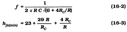
The circuit oscillates only if the BJT current gain is equal to (or larger than) the minimum value determined from Eq. 16-3. With R = RC, a minimum hfe of 56 is required to sustain circuit oscillation. With R = 10 RC, hfe(min) must be greater than 300. The output waveform is likely to be distorted if hfe is substantially greater than the calculated hfe(min). Because hfe varies widely from one transistor to another, RC should be partially adjustable to minimise distortion. Note that in Fig. 16-3, the amplifier input resistance (Zi) constitutes part of the last resistor in the phase shift network.
RC Phase Shift Oscillator using BJT Circuit Diagram:
RC Phase Shift Oscillator using BJT Circuit Diagram design should be approached by first selecting R equal to or greater than the estimated amplifier Zi. Then, RC is selected equal to R, C is calculated from Eq. 16-2, and the rest of the component values are determined for the circuit dc conditions. The impedance of CE should be much lower than hie/(1 + hfe) at the oscillating frequency.