Phase Discriminator:
This Phase Discriminator is also known as the center-tuned discriminator or the Foster-Seeley discriminator, after its inventors. It is possible to obtain the same S-shaped response curve from a circuit in which the primary and the secondary windings are both tuned to the center frequency of the incoming signal. This is desirable because it greatly simplifies alignment, and also because the process yields far better linearity than slope detection. In this new circuit, as shown in Figure 6-36, the same diode and load arrangement is used as in the balanced slope detector because such an arrangement is eminently satisfactory. The method of ensuring that the voltages fed to the diodes vary linearly with the deviation of the input signal has been changed completely. It is true to say that the Foster-Seeley discriminator is derived from the Travis detector.
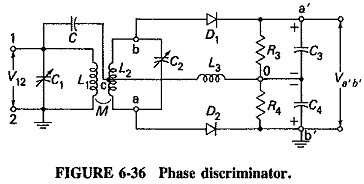
A limited mathematical analysis will now be given, to show that the voltage applied to each diode is the sum of the primary voltage and the corresponding half-secondary voltage. It will also be shown that the primary and secondary voltages are:
- Exactly 90° out of Phase Discriminator when the input frequency is fc
- Less than 90° out of Phase Discriminator when fin is higher than fc
- More than 90° out of Phase Discriminator when fin is below fc
Thus, although the individual component voltages will be the same at the diode inputs at all frequencies, the vector sums will differ with the phase difference between primary and secondary Windings. The result will be that the individual output voltages will be equal only at fc. At all other frequencies the output of one diode will be greater than that of the other. Which diode has the larger output will depend entirely on whether fin is above or below fc. As for the output arrangements, it will be noted that they are the same as in the balanced slope detector. Accordingly, the overall output will be positive or negative according to the input frequency. As required, the magnitude of the output will depend on the deviation of the input frequency from fc.
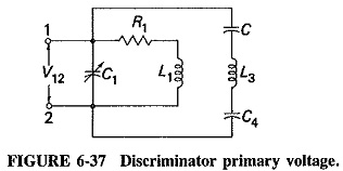
The resistances forming the load are made much larger than the capacitive reactances. It can be seen that the circuit composed of C, L3 and C4 is effectively placed across the primary winding. This is shown in Figure 6-37. The voltage across L3, VL, will then be
L3 is an RF choke and is purposely given a large reactance. Hence its reactance will greatly exceed those of C and C4, especially since the first of these is a coupling capacitor and the second is an RF bypass capacitor. Equation (6-9) will reduce to![]()
The first part of the analysis has been achieved proof that the voltage across the RF choke is equal to the applied primary voltage.
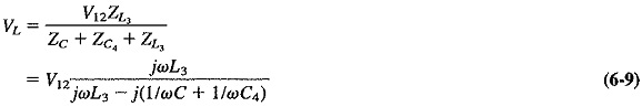
The mutually coupled, double-tuned circuit has high primary and secondary Q and a low mutual inductance. When evaluating the primary current, one may, therefore, neglect the impedance (coupled in from the secondary) and the primary resistance. Then Ip is given simply by

As we recall from basic transformer circuit theory, a voltage is induced in series in the secondary as a result of the current in the primary. This voltage can be expressed as follows:
![]()
where the sign depends on the direction of winding.
It is simpler here to take the connection giving negative mutual induCtance. The secondary circuit is shown in Figure 6-38a, and we have
![]()
The voltage across the secondary winding, Vab, can now be calculated with the aid of Figure 6-38b, which shows the secondary redrawn for this purpose. Then
and may be positive, negative or even zero, depending on the frequency.
The total voltages applied to D1 and D2, Vao and Vbo, respectively, may now be calculated. Therefore

As predicted, the voltage applied to each diode is the sum of the primary voltage and the corresponding half-secondary voltage.
The dc output voltages cannot be calculated exactly because the diode drop is unknown. However, we know that each will be proportional to the peak value of the RF voltage applied to the respective diode:

Consider the situation when the input frequency fin is instantaneously equal to fc. In Equation (6-15), X2 will be zero (resonance) so that Equation (6-14) becomes

From Equation (6-19), it follows that the secondary voltage Vab leads the applied primary voltage by 90°. Thus 1/2 Vab will lead V12 by 90°, and 1/2 Vab, will lag V12
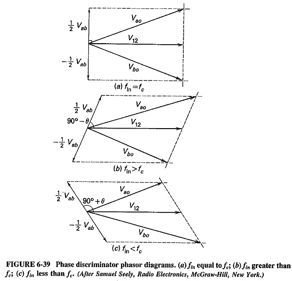
by 90°. It is now possible to add the diode input voltages vectorially, as in Figure 6-39a. It is seen that since Vao = Vbo, the discriminator output is zero. Thus there is no output from this discriminator when the input frequency is equal to the unmodulated carrier frequency, i.e., no output for no modulation. (Actually, this is not a particularly surprising result. The clever part is that at any other frequency there is an output.)
Now consider the case when fin is greater than fc. In Equation (6-15), XL2 is now greater than XC2 so that X2 is positive. Equation (6-14) becomes

From Equation (6-20), it is seen that Vab leads V12 by less than 90° so that – 1/2 Vab must lag V12 by more than 90°. It is apparent from the vector diagram of Figure 6-39 that Vao is now greater than Vbo. The discriminator output will be positive when fin is greater than fc.
Similarly, when the input frequency is smaller than fc, X2 in Equation (6-15) will be negative, and the angle of the impedance Z2 will also be negative. Thus Vab will lead V12 by more than 90°. This time Vao will be smaller than Vbo, and the output voltage Va′b′ will be negative. The appropriate vector diagram is shown in Figure 6-39c.
If the frequency response is plotted for the Phase Discriminator, it will follow the required S shape, as in Figure 6-40. As the input frequency moves farther and farther away from the center frequency, the disparity between the two diode input voltages becomes greater and greater. The output of the discriminator will increase up to the limits of the useful range, as indicated. The limits correspond roughly to the half-power points of the discriminator tuned transformer. Beyond these points, the diode input voltages are reduced because of the frequency response of the transformer, so that the overall output falls.
The Phase Discriminator is much easier to align than the balanced slope detector. There are now only tuned circuits, and both are tuned to the same frequency. Linearity is also better, because the circuit relies less on frequency response and more on the primary-secondary phase relation, which is quite linear. The only defect of this circuit, if it may be called a defect, is that it does not provide any amplitude limiting.