Junction Field Effect Transistor Theory:
n-Channel JFET – The operating principle of an n-channel Junction Field Effect Transistor Theory (JFET) is illustrated by the block representation in Fig. 9-1(a). A piece of n-type semiconductor material, referred to as the channel, is sandwiched between two smaller pieces of p-type (the gates). The ends of the channel are designated the drain (D) and the source (S), and the two pieces of p-type material are connected together and their terminal is named the gate (G).
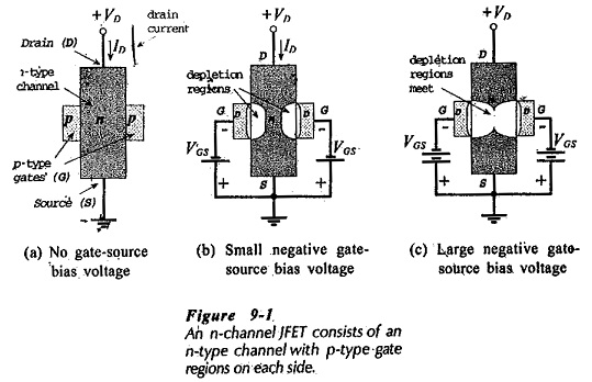
With the gate left unconnected, and a drain-source voltage (VD) applied (positive at the drain, negative at the source), a drain current (ID) flows, as shown in Fig. 9-1(a). When a gate-source voltage (VGS) is applied with the gate negative with respect to the source [Fig. 9-1(b)], the gate-channel pn-junctions are reverse biased. The channel is more lightly doped than the gate material, so the depletion regions penetrate deep into the channel. Because the depletion regions are regions depleted of charge carriers, they behave as insulators. The result is that the channel is narrowed, its resistance is increased, and ID is reduced. When the negative gate-source bias voltage is further increased, the depletion regions meet as the centre of the channel [Fig. 9-1(c)], and ID is cut off.
An ac signal applied to the gate causes the reverse gate-source voltage to increase as the instantaneous level of the signal goes negative, and to decrease when the signal is positive-going. This causes the gate-channel depletion regions to successively widen and decrease. When the signal goes negative, the depletion widen, the channel resistance is increased, and the drain current decreases. As the signal goes positive, the depletion regions recede, the channel resistance is reduced, and the drain current increases. It is seen that the FET gate-source voltage controls the drain current. The gate-channel pit junctions are maintained in reverse bias, so the gate current is normally extremely low; much lower than the base current for a bipolar transistor.
The name, field effect transistor, comes from the fact that the depletion regions in the channel are produced by the electric field at the reverse-biased gate-channel Junction Field Effect Transistor Theory. The term unipolar device is sometimes applied to a FET, because, unlike a bipolar transistor, the current consists of only one type of charge carrier; electrons in the case of an it-channel device.
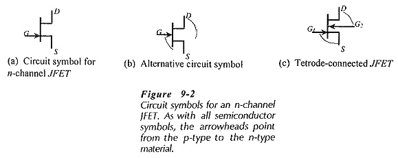
Circuit symbols for an n-channel JFET are shown in Fig. 9-2. As in the case of all semiconductor device symbols, the arrowhead points from p-type to n-type. For an n-channel device, the arrowhead points from the p-type gate to the n-type channel. This is the direction of conventional current flow if the junctions become forward-biased. Some device manufacturers use the symbol in Fig. 9-2(a) with the gate directly opposite the source terminal. Others show the gate centralized between the drain and source [Fig. 9-2(b)). This can sometimes make circuit diagrams confusing unless the drain and source terminals are clearly identified. The symbol in Fig. 9-2(c) is used where the terminals of the two gate regions are provided with separate connecting leads. In this case, the device is referred to as a tetrode-connected FET.
p-Channel JFET:
In a p-channel JFET, shown in block form in Fig. 9-3(a), the channel is p-type semiconductor, and the gates are n-type. The drain-source voltage (VD) is applied negative to the drain, positive to the source, as illustrated, and the drain current flows (in the conventional direction) from source to drain. To reverse-bias the gate-channel junctions, the n-type gate regions must be made positive with respect to the p-type channel. So, the bias voltage is applied positive on the gate terminals, negative on the source.
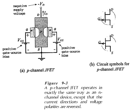
A positive-going signal at the gate terminal of a p-channel JFET increases in the gate-channel junction reverse bias, causing the depletion regions to penetrate further into the channel. This increases the channel resistance and decreases the drain current. Conversely, a negative-going signal narrows the depletion regions, reduces the channel resistance, and increases the drain current.
Circuit symbols for a p-channel JFET are shown in Fig. 9-3(b). The arrowheads again point from the p-type material to the n-type; in this case, from the p-type channel to the n-type gate.
JFET Fabrication and Packaging:
Junction Field Effect Transistor Theory are normally manufactured by the diffusion process. This type of construction is illustrated in Fig. 9-4. Starting with a p-type substrate, an n-channel is diffused, then, p-type impurities are diffused into the channel. Finally, metal terminal connections are deposited through holes in the silicon dioxide surface, as illustrated.
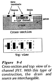
The n-type region is the FET channel, and the two p-type regions constitute the gates. With this symmetrical construction, the drain and source terminals are interchangeable. Other fabrication techniques produce device geometry that is not symmetrical. In these cases, interchanging the drain and source terminals would radically affect the device performance characteristics.
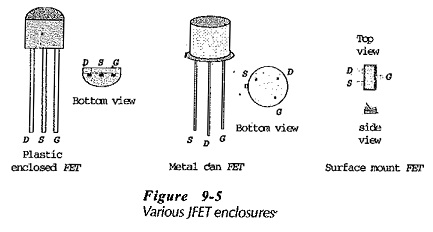
Figure 9-5 shows several FET packages which are similar to BJT enclosures. Note the device terminal identifications in each case.