DC Load Line of BJT Biasing Circuit:
The DC Load Line of BJT Biasing Circuit is a straight line drawn on the transistor output characteristics. For a common-emitter (CE) circuit, the load line is a graph of collector current (IC) versus collector-emitter voltage (VCE), for a given value of collector resistance (RC) and a given supply voltage (VCC). The load line shows all corresponding levels of IC and VCE that can exist in a particular circuit.
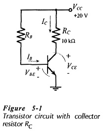
Consider the common-emitter circuit in Fig. 5-1. Note that the polarity of the transistor terminal voltages are such that the base-emitter junction is forward biased and the collector-base junction is reverse biased. These are the normal bias polarities for the transistor junctions. The DC Load Line of BJT Biasing Circuit in Fig. 5-1 is drawn on the device common-emitter characteristics in Fig. 5-2. From Fig. 5-1, the collector-emitter voltage is,
VCE = (supply voltage) – (voltage drop across RC)
![]()
If the base-emitter voltage (VBE) is zero, the transistor is not conducting and IC = 0. Substituting the VCC and RC values from Fig. 5-1 into Eq. 5-1,
![]()
Plot point A on the common-emitter characteristics in Fig. 5-2 at IC = 0 and VCE = 20 V. This is one point on the DC Load Line of BJT Biasing Circuit.
Now assume a collector current of 2 mA, and calculate the corresponding collector-emitter voltage level.
![]()
Plot point B on Fig. 5-2 at VCE = 0 and IC = 2 mA. The straight line drawn through point A and point B is the dc load line for RC = 10 kΩ and VCC = 20 V. If either of these two quantifies is changed, a new load line must be drawn.
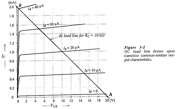
As already stated, the DC Load Line of BJT Biasing Circuit represents all corresponding IC and VCE levels that can exist in the circuit, as represented by Eq. 5-1. For example, a point plotted at VCE = 16 V and IC = 1.5 mA on Fig. 5-2 does not appear on the load line. This combination of voltage and current cannot exist in this particular circuit, (Fig. 5-1). Knowing any one of IB, IC, and VCE, it is easy to determine the other two from a dc load line drawn on the device characteristics.
It is not always necessary to have the device characteristics in order to draw the DC Load Line of BJT Biasing Circuit. A simple graph of IC versus VCE can be used.
DC Bias Point (Q-Point):
The dc bias point, or quiescent point (Q-point) (also known as the dc operating point), identifies the transistor collector current and collector-emitter voltage when there is no input signal at the base terminal. Thus, it defines the dc conditions in the circuit. When a signal is applied to the transistor base, IB varies according to the instantaneous amplitude of the signal. This causes IC to vary, and consequently produces a variation in VCE.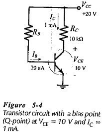
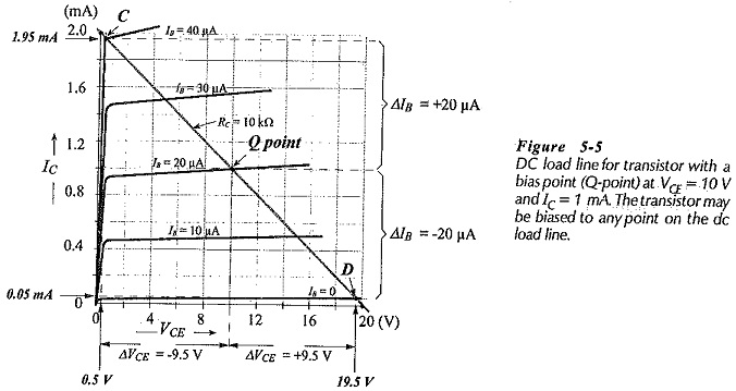
Consider the circuit in Fig. 5-4, and the 10 kΩ load line drawn for the circuit in Fig. 5-5. Assume that the bias conditions are as identified by the Q-point on the load line,
![]()
When IB is increased from 20 μA to 40 μA, IC becomes approximately 1.95 mA and VCE becomes 0.5 V, as illustrated at point Con the load line. The VCE change from the Q-point is,
![]()
So, increasing IB by 20 μA (from 20 μA to 40 μA) caused VCE to decrease by 9.5 V, (from 10 V to 0.5 V).
Now look at the effect of decreasing the base current. When IB is reduced from 20 μA to zero, IC goes down to approximately 0.05 mA, and VCE goes up to 19.5 V (point D on the load line in Fig. 5-5). So, the VCE change is,
![]()
Decreasing IB by 20 μA (From 20 μA to zero) caused VCE to increase by 9.5 V (from 10 V to 19.5 V). It is seen that with the Q-point at IC = 1 mA and VCE = 10 V, an IB variation of ±20 μA produces a collector voltage swing of ΔVCE = ±9.5 V.
The base current does not have to be varied by the maximum amounts discussed above; it can be increased and decreased by smaller amounts. For example, a base current change of ±10 μA (from the Q-point on Fig. 5-5) would produce a collector current change of ±0.5 mA, and a collector-emitter voltage change of ±5 V.
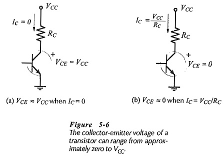
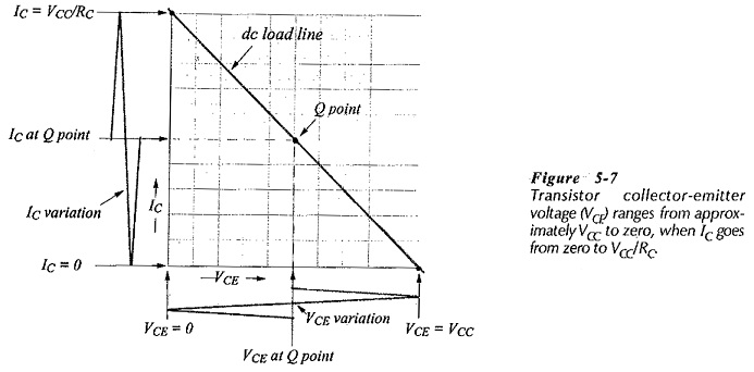
The maximum possible transistor collector-emitter voltage swing for a given circuit can be determined without using the transistor characteristics. For convenience, it may be assumed that IC can be driven to zero at one extreme and to VCC/RC at the other extreme, [see Fig. 5-6]. This changes the collector-emitter voltage from VCE = VCC to VCE = 0, as illustrated in Fig. 5-7. Thus, with the Q-point at the center of the load line, the maximum possible collector voltage swing is seen to be approximately ±VCC/2
Q-point Selection:
Suppose that, instead of being biased half way along the load line, the transistor is biased at IC = 0.5 mA, and VCE = 15 V, as shown in Fig. 5-8(a). Increasing the collector current to 2 mA reduces VCE to zero, giving ΔVCE = -15 V. Reducing IC to zero increases VCE to VCC, producing ΔVCE = +5 V.
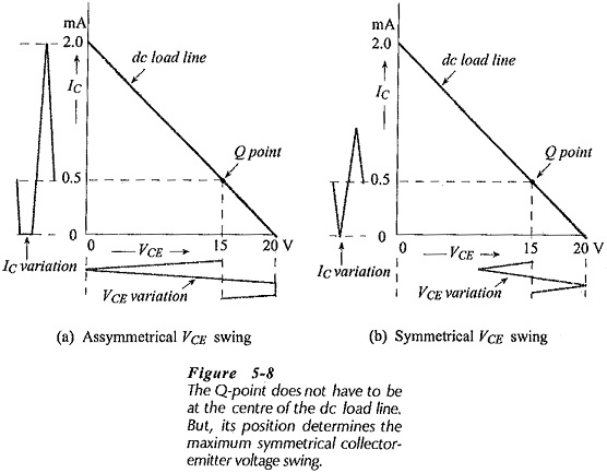
When used as an amplifier, the transistor output (collector-emitter) voltage must swing up and down by equal amounts; that is, the output voltage swing must be symmetrical above and below the bias point. So, the asymmetrical VCE swing of -15 V +5 V illustrated in Fig. 5-8(a) is unsuitable. If IC is driven up and down by ±0.5 mA [see Fig. 5-8(b)], a symmetrical output voltage swing of ±5 V is obtained. This is the maximum symmetrical output voltage swing that can be achieved with the bias point shown in Fig. 5-8.
In many cases circuits are designed to have the Q-point at the center of the load line (as in Figs. 5-5 and 5-7) to give the largest possible symmetrical output voltage swing. This is especially true for some large signal amplifiers. Small signal amplifiers usually require an output voltage swing not greater than ±1 V. So,
Transistors in amplifiers do not all have to be biased at the center of the dc load line.
Effect of Emitter Resistor:
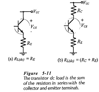
Figure 5-11(a) shows a circuit that has a resistor (RE) in series with the transistor emitter terminal, and the supply voltage connected directly to the collector terminal. In this case RE is the dc load, and Eq. 5-1 is rewritten as,
![]()
The DC Load Line of BJT Biasing Circuit is drawn exactly as discussed, with IE taken as equal to IC for convenience.
In Fig. 5-11(b) collector and emitter resistors RC and RE are both present, and the total dc load in series with the transistor is (RC+ RE). For drawing the DC Load Line of BJT Biasing Circuit, Eq. 5-1 is modified to,
![]()
Note that the voltage drop across the emitter resistor is actually (IE RE), but again for convenience IE is taken as equal to IC.