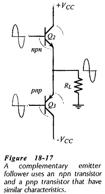
Complementary Emitter Follower Circuit:
Two BJTs connected to function as Complementary Emitter Follower Circuit are shown in Fig. 18-17. Although one is npn and the other is prim the devices are selected to have similar parameters, so they are complementary transistors. The circuit is termed a complementary emitter follower.
A single-transistor emitter follower is essentially a small-signal circuit, because large signals can reverse bias the transistor base-emitter junction when the input polarity is opposite to the transistor VBE polarity.
An npn emitter follower might not correctly reproduce the negative-going portion of a large signal, while a pnp emitter follower might not reproduce the positive-going portion.
Complementary emitter followers have similar signals applied simultaneously to both device bases, as illustrated.
Transistor Q1 conducts during the positive half-cycle of the signal, and it pulls the output voltage up to follow the input. During this time, Q2 base-emitter junction is reverse biased.
For the duration of the negative half-cycle of the input, Q1 base-emitter junction is reversed and Q2 conducts, pulling the output down to follow the input. Thus, the complementary emitter follower is a large-signal circuit with the low output impedance typical of emitter followers.