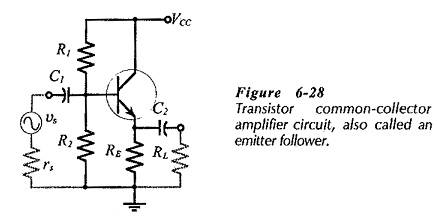
Common Collector Circuit Analysis:
In the Common Collector Circuit Analysis (CC) shown in Fig. 6-28 the external load (RL) is capacitor-coupled to the transistor emitter terminal. The circuit uses voltage divider bias to derive the transistor base voltage (VB) from the supply. The transistor collector terminal is directly connected to VCC, no collector resistor is used. The circuit output voltage is developed across the emitter resistor (RE), and there is no bypass capacitor.
To understand the operation of a Common Collector Circuit Analysis, note that VB is a constant quantity, and that VE = VB – VBE. When a signal is applied via C1 to the transistor base, VB increases and decreases as the signal goes positive and negative. If the signal voltage (vs) increases to +0.5 V, VB is increased by 0.5 V. Also, VE increases by 0.5 V, because VBE remains substantially constant, and VE = VB – VBE. The change in VE is coupled via C2 to give an ac output voltage (vo = 0.5 V), (see the waveforms in Fig. 6-29). Similarly, when vs decreases to -0.5 V, both VB and VE decrease by 0.5 V, giving vo = -0.5 V.
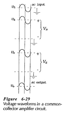
It is seen that the ac output voltage from a CC circuit is essentially the same as the input voltage; there is no voltage gain or phase shift. Thus, the Common Collector Circuit Analysis can be said to have a voltage gain of 1. (Actually, the output voltage can be shown to be slightly smaller than the input because of a very small change in VBE.)
The fact that the CC output voltage follows the changes in signal voltage gives the circuit its other name: emitter follower.
h-Parameter Equivalent Circuit:
As for a CE circuit, the power supply and capacitors must be replaced with short-circuits to study the CC ac performance. This gives the CC ac equivalent circuit in Fig. 6-30(a). The input terminals of the ac equivalent circuit are seen to be the transistor base and collector, and the output terminals are the emitter and collector. Because the collector terminal is common to both input and output, the circuit configuration is named Common Collector Circuit Analysis.
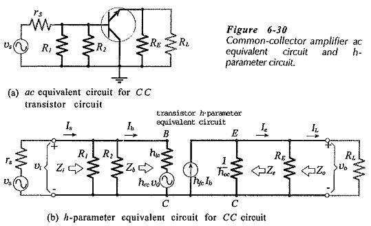
The CC h-parameter circuit is now drawn by substituting the transistor h-parameter model into the ac equivalent circuit, to give the circuit in Fig. 6-30(b). The current directions and voltage polarities indicated in Fig. 6-30(b) are, once again, those that are produced by a positive-going signal voltage. It should be noted that hrc = 1 for a CC circuit; all of vo is fed back to the input. So, unlike the case of a CE circuit, the feedback generator cannot be omitted in the equivalent circuit of a CE amplifier.
Input Impedance:
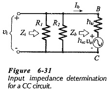
The input impedance for the Common Collector Circuit Analysis is determined by first writing an equation for the input voltage. Referring to Fig. 6-30 and Fig. 6-31,
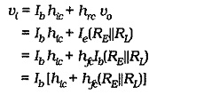
Equation 6-23 is similar to the equation for the transistor input impedance in a CE circuit with an unbypassed emitter resistor (Eq. 6-20), except that RL is now in parallel with RE. The circuit input impedance is again given by Eq. 6-12,![]()
Using Eq. 6-23, the input impedance at the transistor base in a CC circuit can be quickly estimated. A circuit with RE = 1 kΩ and hfe = 100, has Zb ≈ 100 kΩ if RL ≫RE.
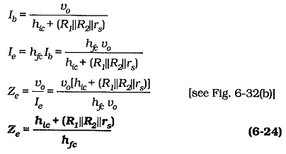
Output Impedance:
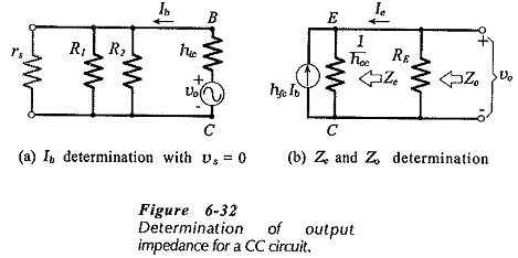
As already discussed, the at voltage at the output of a CC circuit is all fed back to the input. This fact is used in determining the output impedance (Ze) at the emitter terminal. The signal voltage is assumed to be zero, and vo is used to calculate Ie. With vs = 0, Ib is produced by the fed back voltage (hrc vo =vo), [see Fig. 6-32(a)].
Note that the output impedance at the emitter terminal is
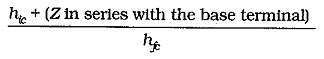
It is interesting to compare this to the base input impedance (Eq. 6-23), which is,![]()
Equation 6-24 gives the device output impedance. (Actually, 1/ hoc should be included, but it has a negligible effect on Ze.) The circuit output impedance also involves RE, [see Fig. 6-32(b)].
![]()
RE is usually much larger than Ze, so that Zo ≈ Ze.
Voltage Gain:
As already explained, the ac output voltage from a CC circuit is almost exactly equal to the input voltage. However, the precise equation for Av is easily derived by considering the ac output and input voltages as derived from Fig, 6-30(b).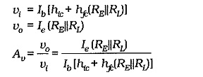
this reduces to,
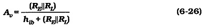
Because r′e ≈ hib, Eq. 6-26 can be used in situations where the device parameters are unknown. Usually, RE || RL is so much larger than hib that the CC circuit voltage gain is simply taken as,
![]()
Summary of CC Circuit Performance:
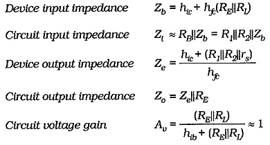
A Common Collector Circuit Analysis has a voltage gain of 1, no phase shift between input and output, high input impedance, and low output impedance. Because of its high Zi, low Zo, and unity gain, the CC circuit is normally used as a buffer amplifier, placed between a high impedance signal source and a low impedance load.