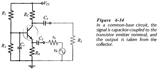
Common Base Circuit Diagram:
The Common Base Circuit Diagram (CB) shown in Fig. 6-34 is very similar to a CE circuit, except that the input signal is applied to the transistor emitter terminal (via C2), instead of the base. Also, there is no bypass capacitor across the RE, but the base terminal is ac grounded via capacitor C1. Because the base is ac grounded, all of the signal voltage is developed across the transistor base-emitter Junction. As for a CE circuit, the output voltage is developed across the collector resistor (RC).
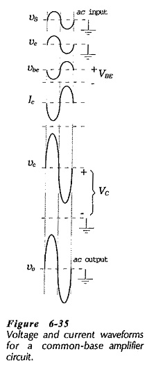
A positive-going signal voltage at the input of a Common Base Circuit Diagram pushes the transistor emitter in a positive direction while the base voltage remains fixed. Thus, a positive-going signal reduced the base-emitter voltage, (see the waveforms in Fig. 6-35). The reduction in VBE reduces the transistor collector current, and the IC reduction reduces VRC, and consequently, causes the transistor collector voltage to increase. The rise in VC is effectively a rise in the circuit output voltage (vo). It is seen that a positive-going input voltage produced a positive-going output. It can also be demonstrated that a negative-going input produces a negative-going output. There is no phase shift from input to output in a Common Base Circuit Diagram.
h-parameter Equivalent Circuit:
The CB ac equivalent circuit is drawn, as always, by replacing the supply voltage and capacitors with short circuits. This gives the circuit in Fig. 6-36(a), which shows that the transistor base terminal (grounded via capacitor C1) is common to both input and output. Hence the name common base.
The CB h-parameter circuit is now drawn by substituting the transistor h-parameter model into the ac equivalent circuit, giving the circuit in Fig. 6-36(b). Once again, the current directions and voltage polarities indicated in the h-parameter circuit are those produced by a positive-going signal voltage. Note that the feedback voltage generator (hrb vo) is not included in the CB h-parameter circuit. This is because the feedback voltage effect is so small that it can be neglected when deriving practical approximate equations for the circuit performance. This corresponds with the CE h-parameter circuit, but not with the CC h-parameter circuit, where the feedback voltage is very important.
Input Impedance:
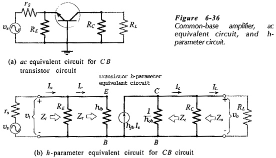
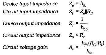
Referring to Fig. 6-36(b), the input impedance to the transistor emitter is simply hib.![]()
Typically hib is around 21 Ω for a low-current transistor. (Also, hib ≈ r′e,) Resistor RE is in parallel with Ze, so the circuit input impedance is,
![]()
RE is usually much larger than Ze, so Zi ≈ Ze.
Output Impedance:
‘Looking into’ the collector-base terminals of the CB h-parameter circuit in Fig. 6-36(b), a very large resistance (1/hob) is seen.
![]()
Once again, Zc is the device output impedance, and the circuit output impedance is RC in parallel with Zc.
![]()
Because Zc is normally much larger than RC,Zo ≈ RC.
As in the case of a CE circuit, the output impedance of a Common Base Circuit Diagram can be determined by just reading the resistance of RC.
Voltage Gain:
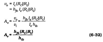
The input voltage equation for the circuit in Fig. 6-36(b) is,
![]()
and the output voltage is,
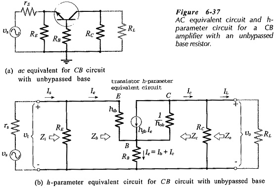
Effect of Unbypassed Base Resistors:
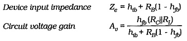
If capacitor C1 is not present in the CB circuit in Fig. 6-34, the transistor base is not ac short-circuited to ground So a resistance (RB = R1||R2) must be shown in the ac equivalent circuit [Fig. 6-37(a)], and in the h-parameter circuit [Fig. 6-37(b)]. The presence of the unbypassed base resistors can substantially affect the transistor input impedance and the circuit voltage gain. Analysis of the h-parameter circuit shows that,
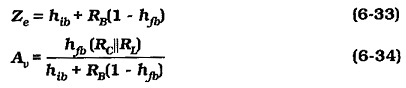
Comparing Eq. 6-33 to Eq. 6-28 (Ze with C1 present), it is seen that RB(1 – hfb) is added to hib to give Ze without C1 present, (Eq. 6-33). Eq. 6-34 is similar to Eq. 6-32 (Av with C1 present), except that RB(1 – hfb) is again added to hib to give the CB circuit voltage gain without C1, (Eq. 6-34). Typically hfb = 0.99 and (1 – hfb) = 0.01.
Summary of CB Circuit Performance:
With the base bypassed to ground:
With the base unbypassed:
A Common Base Circuit Diagram has good voltage gain and relatively high output impedance, like a CE circuit. Unlike a CE circuit, a CB circuit has a very low input impedance, and this makes it unsuitable for most voltage amplifier applications. It is normally employed only as a high-frequency amplifier. The transistor base terminal in a CB circuit should always be bypassed to ground When this is not done, the input impedance is increased and the voltage amplification is substantially reduced.