Collector to Base Bias Circuit:
The Collector to Base Bias Circuit shown in Fig. 5-17(a) has the base resistor (RB) connected between the transistor collector and base terminals. As will be demonstrated, this circuit has significantly improved bias stability for hFE changes compared to base bias.
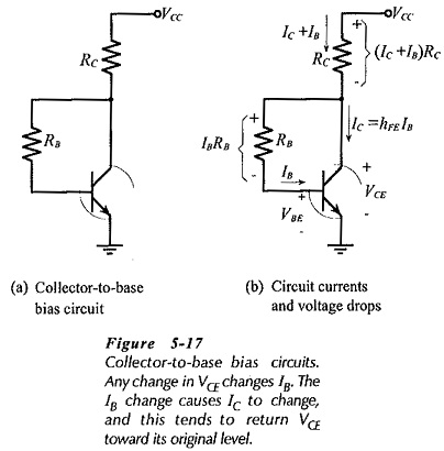
Refer to Fig. 5-17(b) and note that the voltage across RB is dependent on VCE,
Also, VCE is dependent on the level of IC and IB,
![]()
If IC increases above the design level, there is an increased voltage drop across RC, resulting in a reduction in VCE. The reduced VCE level causes IB to be lower than its design level, and because IC = hEE IB, the collector current is also reduced. Thus, an increase in IC produces a feedback effect that tends to return IC toward its original level. Similarly, a reduction in IC produces an increase in VCE which increases IB, thus tending to increase IC back to its original level.
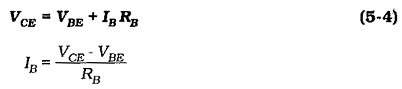
Analysis of this circuit is a little more complicated than base bias analysis. To simplify the process, an equation is first derived for the base current. Substituting for VCE from Eq. 5-4 into Eq. 5-5,
![]()
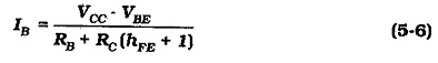
Substituting IC =hFE IB (from Eq. 5-3) into the above equation
![]()
This gives,
Effect of hFE(max) and hFE(min)
As discussed for the base bias circuit, transistors of a given type number have a wide range of hFE values, (hFE spread). This affects the current and voltage levels in all bias circuits. In the Collector to Base Bias Circuit Theory, the feedback from the collector to the base reduces the effects of hFE spread.
It is important to note that, unlike the situation in a base bias circuit, the base current in a collector to base bias circuit does NOT remain constant when the transistor hFE value is changed.
Collector to Base Bias Using a PNP Transistor:
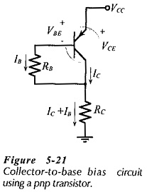
A Collector to Base Bias Circuit Theory using a pnp transistor is illustrated in Fig. 5-21. Note that the voltage polarities and current directions are reversed compared to npn transistor collector to base bias circuit. This circuit can be analysed in exactly the same way as the npn transistor circuit.