BJT Power Amplifier with Op Amp Driver:
BJT Power Amplifier with Op Amp Driver Circuit Operation – The Class-AB power shown in Fig. 18-39 uses an operational amplifier (A1) for the input stage. Resistors R4 and R5 together with the two diodes provide bias for the complementary emitter-follower BJT output stage There is 100% dC negative feedback via R3 to keep the do output at the same level as the op-amp noninverting input, which is grounded via R1. Overall ac negative feedback via R2 and R3 controls the amplifier ac voltage gain.
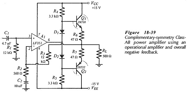
No amplification is produced by the intermediate (output biasing) stage. Instead resistors R4 and R5 provide active pull up for transistors Q1 and Q2. When the op-amp output at the junction of D1 and D2 is increased in a positive direction, A1 supplies current through D2 and R5. So, the voltage drop across R4 is reduced, allowing it to pull the Q1 base up to the required level while supplying increased base current to Q1. This is illustrated by the example voltage levels shown in Fig. 18-40(a). Note that Q2 is biased off when the output voltage is at its positive peak.
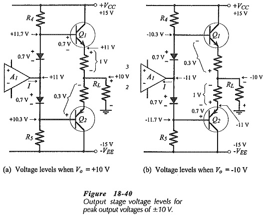
Figure 18-40(b) illustrates the situation when the op-amp output moves in a negative direction. A1 pulls current through R4 and D1, leaving R5 to pull the base of Q2 down to the required voltage level while supplying the increased base current. Transistor Q1 is biased off at this time, as indicated by the example voltage levels.
The circuit in Fig. 18-39 has no provision for adjusting the bias current in the output transistors. However, the diode voltage drops do bias Q1 and Q2 at least into a low-current on state. Although this might not seem enough to completely eliminate cross-over distortion, it should be recalled (from Eq. 13-28) that overall negative feedback (NFB) reduces distortion by a factor of (1+ AvB), where Av is the circuit open-loop gain and B is the feedback factor. Thus, the high open-loop gain of the op-amp severely attenuates the cross-over distortion that would be present without NFB.
Use of Bootstrapping Capacitors:
The resistance of (equal resistors) R4 and R5 (in Fig. 18-39) is limited by the need to supply base current to the output transistors. The calculation of RC is already determined by R4 and R5. Also, there is a need for minimum voltage drop across R4 and R5 to produce the base current. Here again, this is shown already where VRC(min) is the minimum voltage drop across RC. This minimum resistor voltage requirement keeps the amplifier maximum peak output voltage well below the supply voltage level, and thus limits the amplifier efficiency.
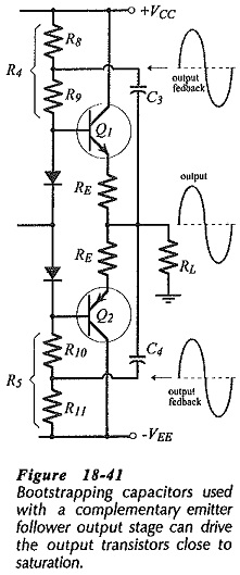
The situation can be substantially improved by the use of the bootstrapping capacitors (C3 and C4) shown in Fig. 18-41. Resistors R4 and R5 are divided into two equal-value resistors (R8 R9 and R10 R11), as illustrated and the capacitors couple the output voltage back to the junctions of these components.
Consider the example supply voltage and dc bias levels shown in Fig. 18-42(a), where the Q1 emitter resistor is left out for simplicity.
The output of A1 is at 0 V, Q3 base is at +0.7 V, and the load voltage is 0 V. The supply voltage is +15 V, the voltage at the junction of R8 and R9 is +7.5 V, and the voltage across C3 is 7.5 V. Note that the voltage drop across R9 is 6.8 V.
The new voltage levels that occur when the op-amp output increases by 3 V are shown in Fig. 18-42(b). Q1 base is at +3.7 V, and the load voltage (Vo) is +3 V. Because C3 is a large capacitor, its terminal voltage remains substantially constant at 7.5 V, so the junction of R8 and R9 is pushed up to;
![]()
With 10.5 V at one end of R9 and 3.7 V at the other end, the voltage across R9 is 6.8 V. This is the same level of VR9 that occurs when the op-amp output is zero. Thus, C3 keeps VR9 constant. Recall that, without the bootstrapping capacitor, VR9 decreases when the op-amp output rises.
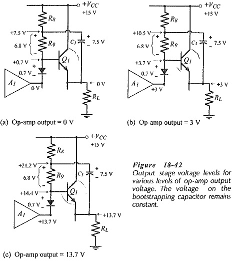
Now consider the voltage levels shown in Fig. 18-42(c), where the op-amp output is +13.7 V. Q1 base voltage is 14.4 V, Vo = +13.7, and the voltage at the R8 R9 junction is,![]()
Once again, VR9 remains constant, however, note that the bootstrapping capacitor has actually driven the R8 R9 junction to a level higher than the supply voltage. This allows the output transistors to be driven into saturation, and the voltage drop across (R8 + R9) is no longer involved in the supply voltage calculation. In this case, the required supply voltage is,
![]()
The peak output voltage can also be limited by the output voltage range of the op-amp. For most op-amps the output voltage range is 1 V to 1.5 V less than the positive and negative supply levels. However, rail-to-rail op-amps are available with an output that ranges from +VCC to -VEE.
Design Procedure:
The BJT Power Amplifier with Op Amp Driver in Fig. 18-44 uses four diodes to forward bias the base-emitter junctions of the Darlington output transistors. Otherwise, the circuit is exactly the same as in Fig. 18-43.
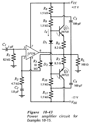
As always, the peak output voltage and current are calculated from the specified output power and load resistance. The supply voltage is determined using Eq. 18-22, and the emitter resistors for the output stage are typically selected as 0.1 RL. The bias network current (I4) should be larger than the peak base current for Q1 and Q2. The resistance of R4 (which equals R8 + R9) is calculated from I4 and the circuit dc voltage drops. R8 should typically be selected as 0.5 R4, and then R9, R10, and R11 are all equal to R8.
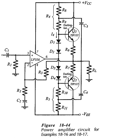
R1 and R3 are equal-value resistors that bias the op-amp input terminals. R2 is calculated from R3 to give the required voltage gain. C2 is selected to have its impedance equal to R2 at the desired lower cutoff frequency (f1). The bootstrapping capacitors are calculated in terms of the resistance in series with them; R8||R9. The op-amp must have a suitable full power bandwidth to produce the peak output voltage at the desired upper cutoff frequency for the BJT Power Amplifier with Op Amp Driver.