BJT Cutoff Frequency and Capacitance:
Device Cutoff Frequency – All transistors have junction capacitances. The junction capacitances and the transit time of charge carriers through the semiconductor material limit the high frequency performance of the device. This limitation is expressed as a cutoff frequency (fα), which is the frequency at which the transistor current gain falls to 0.707 of its gain at low and medium frequencies. The BJT Cutoff Frequency and Capacitance can be expressed in two ways,
- the common emitter cutofff frequency fαe, and
- the common base cutoff frequency (fαb).
fαe is the frequency at which the common emitter current gain (hfe), falls to 0.707 x (mid-frequency hfe). fαb is the frequency at which the common base current gain (hfb) falls to 0.707 x (mid-frequency hfb). It can be shown that,
![]()
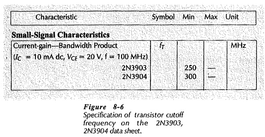
Equation 8-7 shows that fαb can be identified as the current-gainbandwidth product, or total bandwidth (fT). This is the designation used on many transistor data sheets. The data sheet portion in Fig. 8-6 shows that fT is 250 MHz for a 2N3903 and 300 MHz for a 2N3904.
Junction Capacitances:
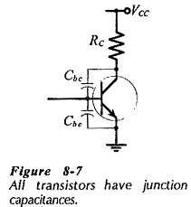
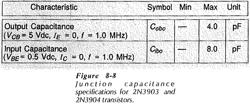
As already discussed, all BJTs have BJT Cutoff Frequency and Capacitance. These are identified as the base-collector capacitance (Cbc) and the base-emitter capacitance (Cbe), (see Fig. 8-7). The device data sheet portion in Fig. 8-8 shows that the capacitances are usually listed as an output capacitance (Cobol, which is the same as Cbc, and an input capacitance (Cibo) which corresponds to Cbe. It should be noted that in both cases, the capacitance values are specified for reverse-biased junctions with zero current levels. Cobo varies when VCB is altered, however, the changes are usually a maximum of approximately ±3 pF. Cibo changes substantially from the specified capacitance when the base-emitter junction is forward biased, (as it always is for linear BJT operation).
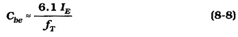
When an emitter current flows across the BE junction, there is a diffusion capacitance at the junction. This is directly proportional to the current level. It can be shown that,
Miller Effect:
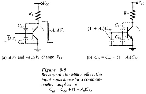
Figure 8-9 shows an input signal (+ΔVi) applied to the base of a transistor connected in CE configuration. If the circuit voltage amplification is -Av, then the collector voltage change is,
![]()
Note that, because of the phase reversal between input and output, the collector voltage is reduced by (Av ΔVi) when the base voltage is increased by ΔVi. The increase in VB and decrease in VC results in a total collector-base voltage reduction of,
![]()
This voltage change appears across the collector-base capacitance. Using the equation Q = C x ΔV, it is found that the charge supplied to the input of the circuit is,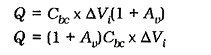
Therefore, “looking into” the base, the collector-base capacitance appears to be (1 + Av)Cbc. So, the capacitance is amplified by a factor of (1 + Av). This is known as the Miller effect.
The total input capacitance (Cin) to the transistor is (1 + Av)Cbc in parallel with the base-emitter capacitance (Cbe);
![]()
It should be noted that the Miller effect occurs only with amplifiers that have a 180° phase shift between input and output, (an inverting amplifier). Consequently, it occurs with CE circuits, but not with CB and emitter follower and circuits.