Biasing Transistor Switching Circuits:
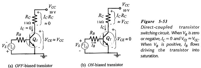
Direct-Coupled Switching Circuit – When a transistor is used as a Biasing Transistor Switching Circuits, it is either biased off to IC = 0, or biased on to its maximum collector current level. Figure 5-53 illustrates the two conditions. Note that the circuit in Fig, 5-53 is termed a direct-coupled switching circuit, because the signal source is directly connected to the circuit. In Fig. 5-53(a) the negative polarity of the base input voltage (VS) biases the transistor (Q1) off. In this case, the only current flowing is the collector base leakage current (ICBO) which is normally so small that it can be neglected.
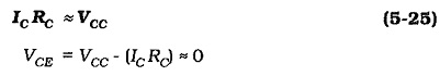
The transistor collector-emitter voltage is,
![]()
With Q1 off [Fig. 5-53(a)],
![]()
In Fig. 5-53(b) VS is positive, and it biases Q1 on to the maximum possible IC level. The collector current is limited only by the collector supply voltage (VCC) and the collector resistor (RC). So,
Now consider Fig. 5-54, which shows the output characteristics and dc load line for the Biasing Transistor Switching Circuits in Fig. 5-53. The load line is drawn by the usual process of plotting point A at (IC= 0 and VCE = VCC), and point B at (VCE = 0 and IC = VCC/RC).
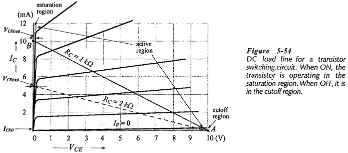
The 1 kΩ load line shows that, when IB = 0, IC is close to zero at,
![]()
At this point the transistor is said to be cut off. The region of the characteristics below IB= 0 is termed the cutoff region. When IC is at its maximum level, the transistor is said to be saturated, and the collector-emitter voltage is the saturation voltage (VCE(sat)).
![]()
The region of the transistor characteristics at (VCE(sat)) is termed the saturation region. The region between saturation and cutoff is the active region, which is where a transistor is normally biased for, amplification. From the load line, it is seen that VCE(sat) is dependent upon the IC level. For the 2 kΩ load line shown dashed in Fig. 5-54, VCE(sat) is smaller than for RC =1 kΩ.
Returning to Fig. 5-53(b), it is seen that IB is a constant quantity,
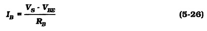
Also, the level of IC depends upon IB,
![]()
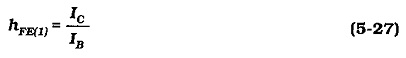
The collector current can be determined from Eq. 5-25 (which assumes that VCE(sat) = 0), and the base current can be calculated from Eq. 5-26. Then, the minimum required current gain for the transistor is,
If the transistor hFE value is less than the calculated hFE(1) value, IC will be lower than the level required for transistor saturation. If the actual hFE of the transistor is greater than the calculated hFE(1), IC tends to be greater than the current level required to saturate the transistor. However, IC cannot exceed VCC/RC. Consequently, an hFE value larger than hFE(1) will adjust down to hFE(1). An hFE value lower than hFE(1) cannot adjust up. So, to ensure that the transistor in a switching circuit saturates, it must have an hFE value equal to or greater than the calculated hFE(1) for the circuit.
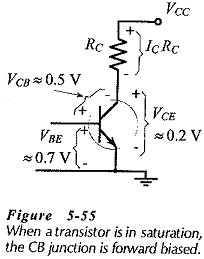
VCE(sat) is typically 0.2 V for a low-current silicon transistor, while VBE is typically 0.7 V. Consider the circuit in Fig. 5-53(b) once again. If VBE = 0.7 V and VCE(sat) = 0.2 V, the transistor base is 0.5 V more positive than the collector,(see Fig. 5-55). This means that the collector-base junction, which is usually reverse biased, is forward biased when the transistor is in saturation. With the collector-base junction forward biased, fewer charge carriers from the emitter are drawn across to the collector, and the device current gain is lower than normal.
Capacitor Coupled Switching Circuit:
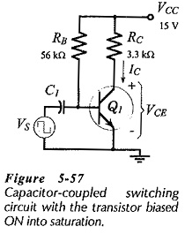
The base bias circuit in Fig. 5-57 is similar to circuits of that type that have already been considered, with the exception that the transistor is biased into saturation. Although too unpredictable for biasing amplifier circuits, base bias is quite satisfactory for Biasing Transistor Switching Circuits. The transistor in Fig. 5-57 is in a normally-on state with VCE = VCE(sat). The capacitor-coupled (pulse waveform) input turns the device off, giving VCE = VCC.
The transistor base current Is
The collector current can be determined From Eq. 5-25, and then the minimum required hFE value can be calculated from Eq. 5-27.
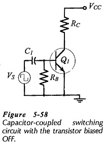
Another type of capacitor-coupled switching circuit is illustrated in Fig. 5-58. In this case, resistor RB keeps the transistor base-emitter voltage at zero, to ensure that the device is in a normally-off state. The capacitor-coupled input voltage biases the transistor on into saturation.
Switching Circuit Design:
The resistance of RC for any one of the Biasing Transistor Switching Circuits discussed can be calculated by using the specified VCC and IC levels with Eq. 5-25. The transistor hFE(min) value can be used with IC to determine the minimum IB level required for transistor saturation. However, concern about the actual transistor current gain can be avoided by using an hFE value of 10. It is very unlikely that the transistor will have an hFE(min) less than 10, so a circuit designed in this way will work with virtually any low-current transistor.
The resistance of RB for the direct-coupled circuit in Fig. 5-53 is calculated from Eq. 5-26. For the normally-on capacitor-coupled circuit in Fig. 5-57, Eq. 5-28 is used for determining the RB value.
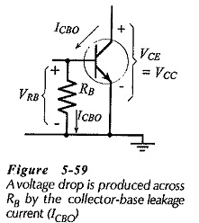
A different approach must be taken for calculating a suitable resistance for RB in the normally-off capacitor-coupled circuit in Fig. 5-58. The current that flows through RB when the transistor is off, and the allowable voltage drop across RB must be considered, (see Fig. 5-59). The resistor current is the collector-base leakage current (ICBO), and the maximum voltage drop produced by ICBO must be much smaller than the normal transistor VBE level when the device is on. ICBO at maximum transistor temperature is unlikely to exceed 5 μA, and a VRB of 0.1 V will normally keep the transistor biased off. So, a maximum resistance value for RB is,
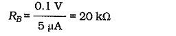
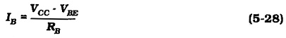
Typically, an RB value of 22 kΩ or lower is suitable for keeping the transistor biased off.