All Pass Filter Design:
The All Pass Filter Design is one that passes all frequency components of the input signal without attenuation. Any ordinary wire can be used to perform this characteristic but the most important factor in an all pass filter is that it provides predictable phase shifts for different frequencies of the input signal.
These All Pass Filter Design are widely used in communications. For example, when signals are transmitted over transmission lines, such as telephone wires, from one point to another, they undergo a change in phase. All pass filters are used to compensate for these phase changes. They are also called delay equalizers or phase correctors.
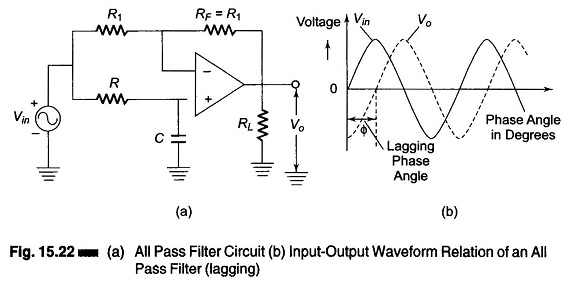
Figure 15.22 shows an all pass filter with the output lagging the input. The output voltage Vo of the filter can be obtained by using the superposition theorem, as follows. From Fig. 15.22(a), we see that
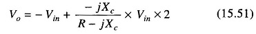
Where
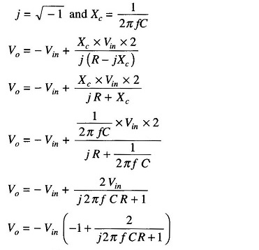
Therefore
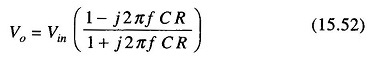
The above equation indicates that the amplitude of Vo/Vin is unity, that is IVoI = |Vin| throughout the useful frequency range and the phase shift between Vo and Vin is a function of input frequency f. The phase angle Φ is given by
![]()
where
- Φ = phase in degrees
- f = frequency in Hz
- R = resistance in Ω
- C = capacitance in F
Referring to Fig. 15.22(a), if the positions of R and C are interchanged, the phase shift between input and output becomes positive. That is, output Vo leads input Vin.